Samsung developing HBM for mobile AI devices
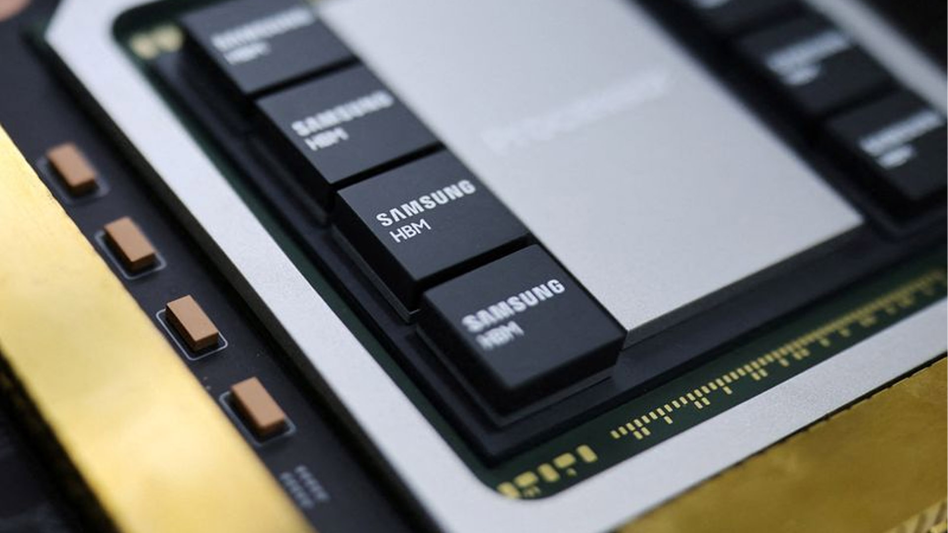
💡Samsung's move to bring HBM to mobile could unlock true on-device LLM performance for developers.
⚡ 30-Second TL;DR
What Changed
Samsung is adapting server-grade HBM technology for mobile form factors.
Why It Matters
This shift could significantly reduce latency for on-device LLMs and improve privacy by keeping data processing local. It marks a major step in hardware-level AI acceleration for mobile ecosystems.
What To Do Next
Monitor Samsung's upcoming mobile SoC specifications for integrated memory bandwidth improvements to optimize your on-device model deployment.
Key Points
- •Samsung is adapting server-grade HBM technology for mobile form factors.
- •Focus on enabling high-performance on-device AI processing.
- •Utilizing complex packaging techniques to integrate HBM into mobile chips.
🧠 Deep Insight
Web-grounded analysis with 11 cited sources.
🔑 Enhanced Key Takeaways
- •Samsung is developing a 'multi-layer stacked FOWLP' technology, which combines ultra-high aspect ratio copper pillars with Fan-Out Wafer Level Packaging (FOWLP) to integrate HBM into mobile devices.
- •This new packaging technology aims to increase bandwidth by 15-30% and enable over 1.5 times the number of memory stacks compared to traditional mobile DRAM.
- •Unlike traditional mobile DRAM (LPDDR) that relies on copper wire bonding with limited I/O terminals (128-256 range) leading to signal loss and heat, HBM's stacked architecture and Through-Silicon Via (TSV) interconnects offer a much wider and more direct data path.
- •The adoption of HBM for mobile devices faces significant engineering challenges, including higher manufacturing costs, the complexity of 3D stacking, lower production yields, and stringent thermal management requirements within the compact and power-constrained mobile form factor.
- •Industry insiders predict that this advanced mobile HBM technology may debut in subsequent versions of Samsung's Exynos 2800 or Exynos 2900 mobile processors.
🛠️ Technical Deep Dive
- Samsung's mobile HBM solution utilizes 'multi-layer stacked FOWLP' packaging, which is an advancement of its existing Vertical Copper Post Stack (VCS) technology.
- The aspect ratio of copper pillars in VCS packaging has been significantly increased from the previous 3-5:1 to 15-20:1 to enhance bandwidth.
- Fan-Out Wafer Level Packaging (FOWLP) is integrated to provide structural integrity and support for ultra-high aspect ratio copper pillars, especially when their diameter falls below 10 micrometers, preventing bending or breakage.
- FOWLP also contributes to increasing the number of I/O terminals, further boosting overall bandwidth.
- HBM employs 3D stacking of DRAM dies interconnected by thousands of microscopic Through-Silicon Vias (TSVs), which dramatically shortens data travel distance and creates a massively wide data bus to the processor.
- Samsung holds a patent portfolio related to extending HBM's utility for AI inference, including Processing-in-Memory (PIM) capabilities, where a logic circuit can convert host commands into PIM commands to execute computation directly within the memory stack.
- Key challenges for mobile HBM include managing power consumption and heat dissipation within the tight thermal budget of mobile devices.
🔮 Future ImplicationsAI analysis grounded in cited sources
⏳ Timeline
📎 Sources (11)
Factual claims are grounded in the sources below. Forward-looking analysis is AI-generated interpretation.
Weekly AI Recap
Read this week's curated digest of top AI events →
👉Related Updates




AI-curated news aggregator. All content rights belong to original publishers.
Original source: cnBeta (Full RSS) ↗