Samsung and SK Hynix Delay HBM4 Hybrid Bonding
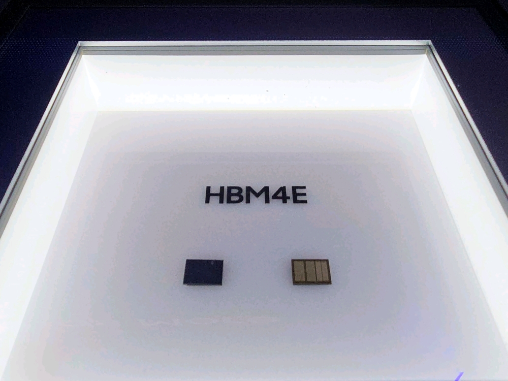
💡Crucial supply chain update for AI hardware architects tracking HBM memory performance and roadmap.
⚡ 30-Second TL;DR
What Changed
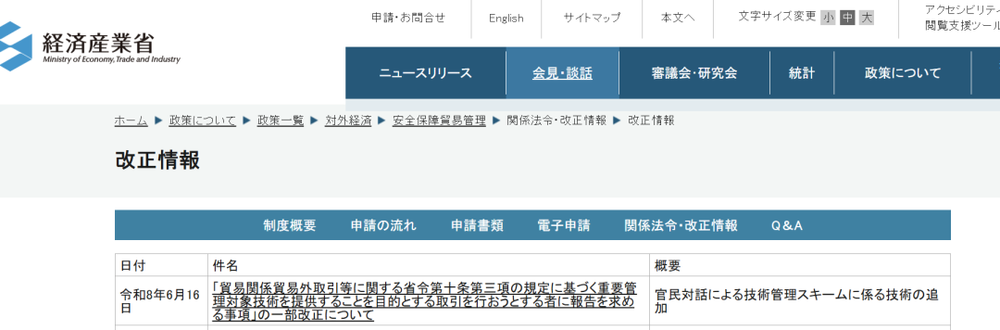
JEDEC 放寬 HBM 堆疊厚度規範
Why It Matters
This delay may impact the performance scaling of next-generation AI accelerators that rely on HBM4 for memory bandwidth. It suggests that the industry is prioritizing yield and standard compliance over aggressive architectural changes.
What To Do Next
Adjust your hardware roadmap expectations for AI accelerator performance, accounting for a potential delay in HBM4 bandwidth improvements.
Key Points
- •JEDEC 放寬 HBM 堆疊厚度規範
- •Samsung 與 SK Hynix 將混合鍵合推遲至 HBM4E
- •記憶體封裝技術路線圖面臨調整
🧠 Deep Insight
AI-generated analysis for this event — not the original article.
🔑 Enhanced Key Takeaways
- •The relaxation of JEDEC standards allows for a total stack height of 775 micrometers for HBM4, up from the previous 720-micrometer target, reducing the immediate pressure to implement hybrid bonding.
- •Thermal management challenges in 16-high HBM4 stacks remain a primary driver for the eventual transition to hybrid bonding in the HBM4E generation.
- •Micron Technology is also recalibrating its HBM4 roadmap, potentially aligning with the industry-wide shift to prioritize yield stability over early adoption of advanced bonding techniques.
- •The delay in hybrid bonding adoption is expected to extend the lifecycle of current Thermocompression Non-Conductive Film (TC-NCF) and Mass Reflow Molded Underfill (MR-MUF) packaging methods.
- •Foundry partners, particularly TSMC, are adjusting their CoWoS (Chip-on-Wafer-on-Substrate) capacity planning to accommodate the continued use of traditional bonding methods for initial HBM4 production.
📊 Competitor Analysis▸ Show
| Feature | Samsung (HBM4) | SK Hynix (HBM4) | Micron (HBM4) |
|---|---|---|---|
| Bonding Tech (Initial) | TC-NCF | MR-MUF | TC-NCF |
| Hybrid Bonding Target | HBM4E | HBM4E | HBM4E |
| Stack Height (JEDEC) | 775μm | 775μm | 775μm |
🛠️ Technical Deep Dive
- Hybrid bonding replaces traditional micro-bumps with direct copper-to-copper interconnects, significantly increasing I/O density.
- The transition to hybrid bonding is critical for achieving the vertical pitch scaling required for 16-high stacks and beyond.
- TC-NCF (Thermal Compression Non-Conductive Film) utilizes a film-based adhesive to protect interconnects during bonding, favored by Samsung for its thermal management properties.
- MR-MUF (Mass Reflow Molded Underfill) involves reflowing solder bumps in a single process step, favored by SK Hynix for its high throughput and yield efficiency.
🔮 Future ImplicationsAI analysis grounded in cited sources
⏳ Timeline
Weekly AI Recap
Read this week's curated digest of top AI events →
👉Related Updates


AI-curated news aggregator. All content rights belong to original publishers.
Original source: cnBeta (Full RSS) ↗
This is a summary, not the original. Read the source, or get the weekly briefing.
Weekly AI briefing
One email a week. Unsubscribe anytime.