Resonac Proves Japan's AI Chip Backend Edge
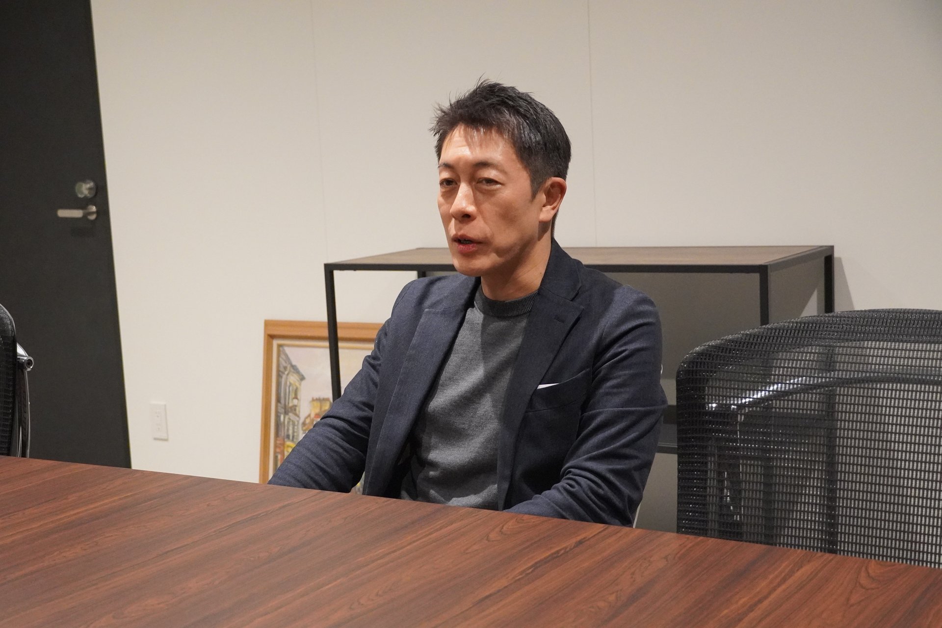
💡Japan's backend materials secure Big Tech's AI chip pipeline
⚡ 30-Second TL;DR
What Changed
AI chip demand surges with gen AI boom
Why It Matters
Ensures stable AI chip supply for big tech, positioning Japanese firms like Resonac as key partners. Could mitigate global shortages in advanced semiconductor production.
What To Do Next
Reach out to Resonac for co-development partnerships on AI semiconductor backend materials.
Key Points
- •AI chip demand surges with gen AI boom
- •Backend materials vital for complex structures
- •Resonac excels via co-creation development approach
- •Highlights Japan's supply chain strengths
🧠 Deep Insight
AI-generated analysis for this event — not the original article.
🔑 Enhanced Key Takeaways
- •Resonac's co-creation strategy centers on its 'Packaging Solution Center' (PSC), which facilitates rapid prototyping and material testing in collaboration with global chipmakers and equipment manufacturers.
- •The company has successfully commercialized advanced materials for 2.5D and 3D packaging, specifically focusing on high-performance thermal interface materials (TIMs) and photosensitive insulating films required for chiplet architectures.
- •Resonac is leveraging its legacy as a chemical conglomerate to integrate the entire backend material supply chain, reducing the time-to-market for next-generation AI semiconductor packaging solutions.
📊 Competitor Analysis▸ Show
| Feature | Resonac | JSR Corporation | Shin-Etsu Chemical |
|---|---|---|---|
| Core Focus | Backend packaging materials & co-creation | Photoresists & advanced lithography | Silicon wafers & packaging materials |
| AI Strategy | Integrated packaging solutions | Material purity for EUV | High-purity materials for 3D stacking |
| Market Position | Leader in backend integration | Leader in lithography materials | Dominant in wafer supply |
🛠️ Technical Deep Dive
- Thermal Interface Materials (TIMs): Development of high-thermal-conductivity materials designed to manage the extreme heat density of AI accelerators (GPUs/TPUs) in 3D-stacked configurations.
- Photosensitive Insulating Films: Advanced dielectric materials that enable high-density wiring and fine-pitch interconnects essential for chiplet-based architectures.
- Co-creation Infrastructure: Utilization of specialized cleanroom facilities that simulate customer backend processes to validate material performance under real-world manufacturing conditions.
🔮 Future ImplicationsAI analysis grounded in cited sources
⏳ Timeline
Weekly AI Recap
Read this week's curated digest of top AI events →
👉Related Updates

AI-curated news aggregator. All content rights belong to original publishers.
Original source: ITmedia AI+ (日本) ↗
This is a summary, not the original. Read the source, or get the weekly briefing.
Weekly AI briefing
One email a week. Unsubscribe anytime.