Razor Lake May Bring Intel a Massive Cache Boost
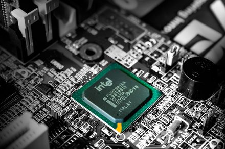
💡A potential cache leap could reshape performance expectations for laptop-based local AI inference.
⚡ 30-Second TL;DR
What Changed
Razor Lake mobile CPUs may adopt bLLC for larger cache pools.
Why It Matters
Larger on-chip caches could improve performance and efficiency for local AI inference and other memory-sensitive workloads. However, the claims remain unconfirmed, and the unclear process designation makes performance and availability difficult to assess.
What To Do Next
Track Razor Lake benchmark and platform disclosures before planning laptop-based local inference deployments around its rumored cache advantages.
Key Points
- •Razor Lake mobile CPUs may adopt bLLC for larger cache pools.
- •The cache expansion could improve data access for laptop workloads.
- •The reported manufacturing process has shifted from TSMC N2X to N2P V2.
🧠 Deep Insight
AI-generated analysis for this event.
🔑 Enhanced Key Takeaways
- •bLLC (backside Level-Last Cache) is reportedly designed to decouple cache memory from the primary logic die, allowing for higher density without increasing the footprint of the compute cores.
- •The shift to TSMC N2P V2 suggests Intel is prioritizing power efficiency and transistor density optimization over the raw performance-per-watt focus of the N2X node.
- •Industry analysts suggest Razor Lake is intended to compete directly with AMD's 3D V-Cache mobile implementations by providing a more flexible, modular cache architecture.
- •The implementation of bLLC is expected to reduce latency for memory-intensive AI inference tasks running locally on mobile devices.
- •Reports indicate that Razor Lake will utilize a disaggregated chiplet design, separating the CPU compute tiles from the massive cache tiles to improve manufacturing yields.
📊 Competitor Analysis▸ Show
| Feature | Intel Razor Lake (Rumored) | AMD Ryzen 'Zen 6' Mobile | Apple M5 Pro/Max |
|---|---|---|---|
| Cache Tech | bLLC (Backside Cache) | 3D V-Cache | Unified Memory Architecture |
| Process Node | TSMC N2P V2 | TSMC N2P | TSMC N3P / N2 |
| Primary Focus | Mobile AI/Cache Density | Gaming/Efficiency | Performance/Efficiency |
🛠️ Technical Deep Dive
- bLLC Architecture: Utilizes backside power delivery networks to integrate cache layers directly beneath the logic, minimizing signal path distance.
- N2P V2 Process: An iteration of TSMC's 2nm class nodes focusing on improved gate-all-around (GAA) transistor performance and reduced leakage compared to N2.
- Cache Scaling: Expected to support L4 cache capacities exceeding 128MB in mobile form factors, significantly higher than current standard mobile CPU cache pools.
- Interconnect: Likely employs advanced packaging technologies (Foveros or similar) to manage the high-bandwidth communication between the compute die and the bLLC die.
🔮 Future ImplicationsAI analysis grounded in cited sources
⏳ Timeline
Weekly AI Recap
Read this week's curated digest of top AI events →
👉Related Updates

AI-curated news aggregator. All content rights belong to original publishers.
Original source: Digital Trends ↗