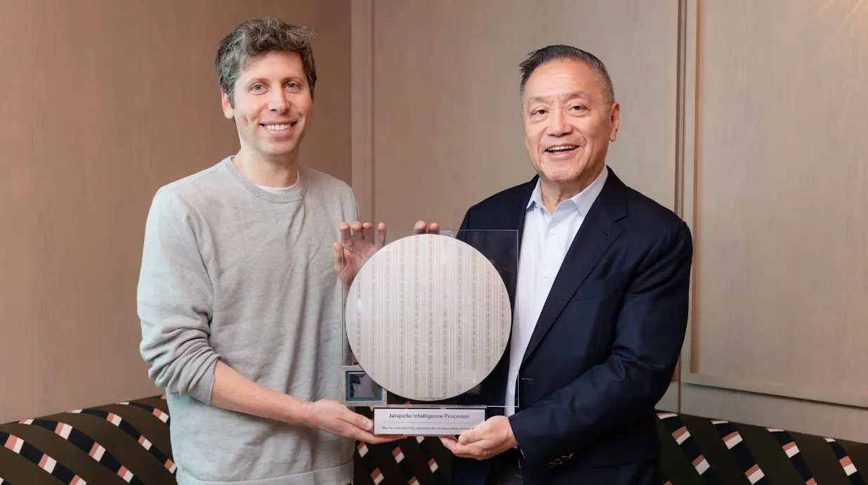
OpenAI and Broadcom launch custom AI chip Jalapeño
💡OpenAI's first custom chip signals a major move to reduce Nvidia dependency and optimize inference costs.
⚡ 30-Second TL;DR
What Changed
Jalapeño is designed specifically for AI inference workloads
Why It Matters
This move marks a significant shift in OpenAI's infrastructure strategy, moving toward vertical integration to control costs and performance. It poses a long-term competitive threat to Nvidia's dominance in the AI hardware market.
What To Do Next
Evaluate how custom silicon like Jalapeño might influence future API latency and cost structures for your AI applications.
🧠 Deep Insight
AI-generated analysis for this event.
🔑 Enhanced Key Takeaways
- •The Jalapeño chip utilizes a 2nm process node, marking a significant shift toward high-density, power-efficient silicon for large-scale inference.
- •Broadcom's role centers on providing the SerDes (Serializer/Deserializer) technology and custom ASIC design services to ensure high-bandwidth interconnects between chip clusters.
- •The architecture incorporates a specialized 'Transformer Engine' block designed to accelerate attention mechanism calculations, which are the primary bottleneck in LLM inference.
- •OpenAI is reportedly integrating Jalapeño into its 'Orion' infrastructure, aiming to reduce the total cost of ownership (TCO) for inference by approximately 40% compared to off-the-shelf GPU solutions.
- •The project involved a multi-year collaboration that included TSMC as the primary foundry partner, ensuring supply chain diversification away from reliance on standard H100/B200 allocations.
📊 Competitor Analysis▸ Show
| Feature | OpenAI Jalapeño | NVIDIA Blackwell (B200) | Google TPU v6p |
|---|---|---|---|
| Primary Focus | Inference Optimization | Training & Inference | Large-scale Training |
| Architecture | Custom ASIC (Inference) | GPU (General Purpose) | ASIC (TPU) |
| Interconnect | Proprietary Fabric | NVLink | ICI (Inter-Chip Interconnect) |
| Pricing | Internal Cost (Estimated) | Market Premium | Cloud Service Pricing |
🛠️ Technical Deep Dive
- Architecture: Custom ASIC optimized for Transformer-based inference workloads.
- Process Node: 2nm fabrication process (TSMC).
- Memory: Integrated HBM3e stacks to maximize memory bandwidth for large model weights.
- Interconnect: High-speed SerDes integration for low-latency communication in multi-chip clusters.
- Optimization: Dedicated hardware blocks for FP8 and INT8 quantization to improve throughput for ChatGPT and agentic tasks.
🔮 Future ImplicationsAI analysis grounded in cited sources
⏳ Timeline
📰 Event Coverage
Weekly AI Recap
Read this week's curated digest of top AI events →
👉Related Updates

AI-curated news aggregator. All content rights belong to original publishers.
Original source: cnBeta (Full RSS) ↗