🔥36氪•Stalecollected in 54m
Nvidia Rubin Kicks Off M10 Testing

💡Nvidia Rubin PCB tests herald 2027 AI infra upgrade cycle.
⚡ 30-Second TL;DR
What Changed
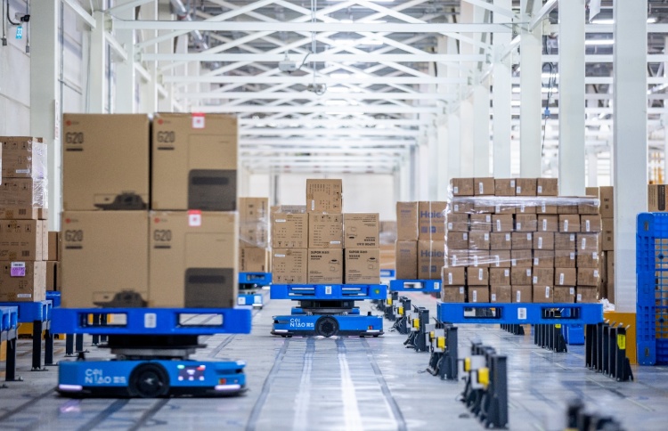
Nvidia testing M10 CCL with PCB vendors
Why It Matters
Signals Nvidia's aggressive AI hardware roadmap, boosting supply chain for high-end PCBs. AI practitioners can anticipate better server performance and availability post-2027.
What To Do Next
Contact PCB vendors like suppliers of M10 CCL to prepare for Rubin-era AI server builds.
Who should care:Enterprise & Security Teams
🧠 Deep Insight
Web-grounded analysis with 7 cited sources.
🔑 Enhanced Key Takeaways
- •Rubin GPU features two reticle-size compute dies on TSMC 3nm process with two I/O tiles, delivering 50 PFLOPs of dense FP4 compute using 224 Streaming Multiprocessors and fifth-generation Tensor Cores[1][3][5].
- •Rubin Ultra configuration includes 16 stacks of HBM4E (1024GB capacity) and a row of four reticle-sized GPUs with two I/O chiplets, achieving 100 PFLOPs FP4 and 3600W TDP[1][2][7].
- •Rubin platform introduces NVIDIA Vera 88-core Arm-compatible CPU with 1.5TB LPDDR per CPU, NVLink 6 at 3.6TB/s bidirectional, and Kyber rack architecture for enhanced scale-up[1][3][4].
🛠️ Technical Deep Dive
- •Rubin GPU: Two TSMC 3nm reticle-size compute dies + two I/O chiplets; 288GB HBM4 (up to 22TB/s bandwidth); 224 SMs with 5th-gen Tensor Cores for NVFP4/FP8; 50 PFLOPs dense FP4 compute[1][3][6].
- •Rubin Ultra: Four TSMC 3nm reticle-size GPU chiplets + two I/O chiplets; 1024GB HBM4E (32TB/s bandwidth); 100 PFLOPs dense FP4; 3600W TDP requiring extreme cooling[1][2].
- •NVLink 6: 224G SerDes, 3.6TB/s bidirectional GPU-to-GPU bandwidth (doubling lanes from prior gen); supports NVLink-C2C for chip-to-chip[1][3].
- •Vera CPU: 88 custom Olympus Armv9.2 cores; up to 1.2TB/s LPDDR5X bandwidth; NVLink-C2C connectivity; optimized for agentic reasoning and confidential computing[3][4][6].
- •Platform features: 3rd-gen Transformer Engine with adaptive compression; 2nd-gen RAS engine for rack-scale resiliency; modular cable-free trays (18x faster service vs Blackwell)[4][6].
🔮 Future ImplicationsAI analysis grounded in cited sources
Rubin platform reduces inference token cost by up to 10x vs Blackwell
Extreme codesign across Vera CPU, Rubin GPU, NVLink 6, and supporting chips optimizes AI workloads for transformer-era efficiency[4].
AI server PCB upgrade cycle driven by orthogonal backplanes and switch blade boards will peak in 2027 H2
M10 CCL testing targets these advanced interconnects for Rubin Ultra and Feynman, necessitating new procurement amid NVLink lane doubling[1].
Kyber rack and Vera CPUs enable 365TB fast memory per rack
Combines 147TB HBM with 218TB LPDDR across 144 Vera CPUs, supporting gigascale inference context storage[1].
⏳ Timeline
2025-03
NVIDIA announces Rubin platform at GTC 2025 with Vera CPU, Rubin GPU, and NVLink 6 details[1][4]
2025-11
Rubin microarchitecture formalized with 50 PFLOPs FP4 specs and HBM4 integration[5]
2026-03
Nvidia initiates M10 CCL testing for Rubin Ultra and Feynman backplanes with PCB vendors[article]
📎 Sources (7)
Factual claims are grounded in the sources below. Forward-looking analysis is AI-generated interpretation.
- newsletter.semianalysis.com — Nvidia Gtc 2025 Built for Reasoning Vera Rubin Kyber Cpo Dynamo Inference Jensen Math Feynman
- Tom's Hardware — Nvidia Enterprise Roadmap Rubin Rubin Ultra Feynman and Silicon Photonics
- developer.nvidia.com — Inside the Nvidia Rubin Platform Six New Chips One AI Supercomputer
- nvidianews.nvidia.com — Rubin Platform AI Supercomputer
- en.wikipedia.org — Rubin (microarchitecture)
- NVIDIA — Rubin
- naddod.com — Vera Rubin Superchip Transformative Force in Accelerated AI Compute
📰
Weekly AI Recap
Read this week's curated digest of top AI events →
👉Related Updates
AI-curated news aggregator. All content rights belong to original publishers.
Original source: 36氪 ↗