🇨🇳cnBeta (Full RSS)•Stalecollected in 16h
NVIDIA Feynman Debuts 1.6nm A16 GPU Core
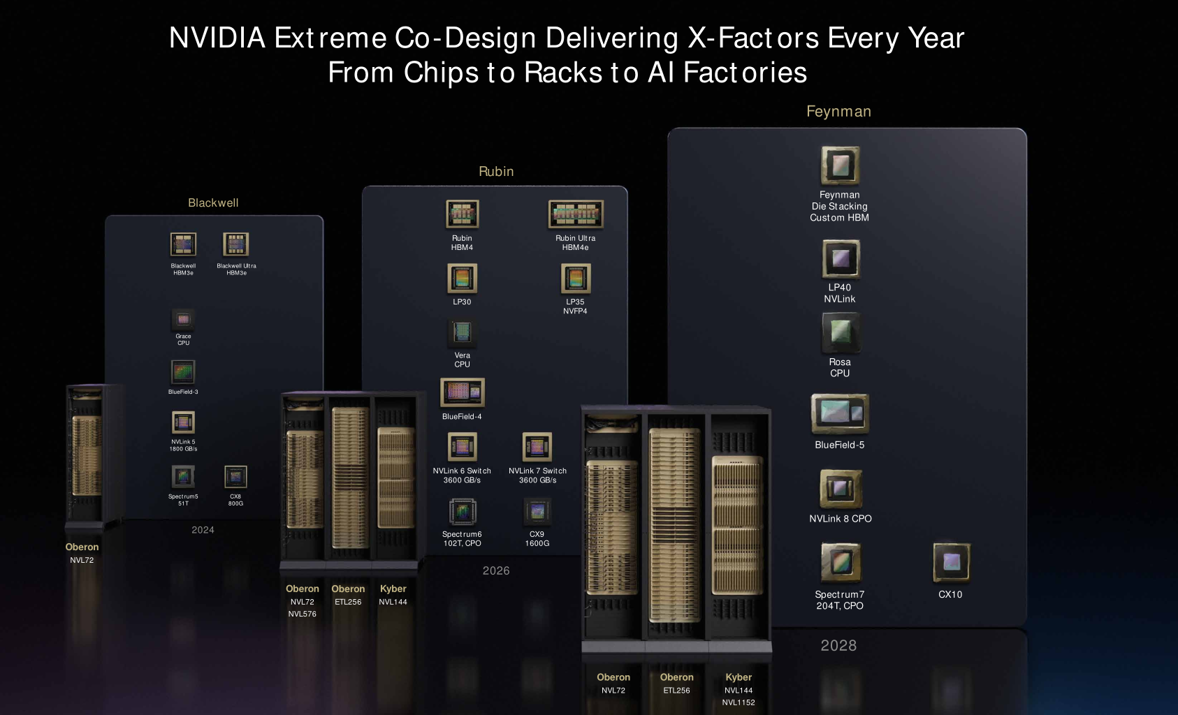
💡NVIDIA's 1.6nm Feynman roadmap signals huge leaps in AI GPU performance and density.
⚡ 30-Second TL;DR
What Changed
Feynman architecture launches in 2028
Why It Matters
Advanced nodes and 3D stacking will enable massive AI compute density gains, but supply limits may hinder rapid scaling of next-gen training clusters.
What To Do Next
Evaluate TSMC A16 roadmap timelines for planning 2028 AI GPU procurement budgets.
Who should care:Enterprise & Security Teams
Key Points
- •Feynman architecture launches in 2028
- •GPU core first to use TSMC 1.6nm A16 process
- •Custom HBM chips and 3D die stacking introduced
- •3nm mixed in due to A16 capacity shortages
🧠 Deep Insight
AI-generated analysis for this event.
🔑 Enhanced Key Takeaways
- •The Feynman architecture marks NVIDIA's transition to a 'disaggregated' chiplet design, moving away from monolithic dies to optimize yield and thermal management for the 1.6nm process.
- •NVIDIA is reportedly partnering with SK Hynix and Micron for the custom HBM integration, specifically targeting HBM4e standards to support the increased memory bandwidth requirements of the Feynman core.
- •The decision to mix 3nm nodes is driven by TSMC's A16 capacity being heavily prioritized for Apple's 2027-2028 mobile silicon roadmap, forcing NVIDIA to adopt a hybrid manufacturing strategy.
📊 Competitor Analysis▸ Show
| Feature | NVIDIA Feynman (A16) | AMD Instinct MI400 Series | Intel Falcon Shores |
|---|---|---|---|
| Process Node | TSMC 1.6nm (A16) | TSMC 2nm / 3nm | Intel 18A / TSMC Hybrid |
| Memory | Custom HBM4e | HBM4 | HBM4 |
| Architecture | Disaggregated Chiplet | CDNA Next | XPU Hybrid |
🛠️ Technical Deep Dive
- •A16 Process: Utilizes TSMC's Super Power Rail (SPR) technology, which moves power delivery to the backside of the wafer, significantly reducing IR drop and improving logic density compared to N2P.
- •3D Die Stacking: Employs an advanced CoWoS-L (Chip-on-Wafer-on-Substrate) variant to integrate the 1.6nm compute tiles with 3nm I/O dies and HBM stacks.
- •Power Delivery: The architecture features a redesigned power delivery network (PDN) to handle the extreme current density required by the A16 logic gates, mitigating thermal throttling risks.
🔮 Future ImplicationsAI analysis grounded in cited sources
NVIDIA will face significant gross margin pressure in 2028 due to the high cost of A16 wafers and complex packaging.
The combination of TSMC's premium A16 pricing and the yield overhead of 3D-stacked chiplets will substantially increase the bill of materials per unit.
The Feynman architecture will trigger a industry-wide shift toward backside power delivery in high-performance AI accelerators.
NVIDIA's adoption of A16 validates the necessity of backside power delivery to overcome the physical scaling limits of traditional front-side power distribution.
⏳ Timeline
2024-04
TSMC announces A16 process technology for 2026 production.
2025-03
NVIDIA confirms development of next-generation GPU architecture post-Blackwell.
2026-03
NVIDIA officially unveils Feynman architecture roadmap at GTC.
📰
Weekly AI Recap
Read this week's curated digest of top AI events →
👉Related Updates
AI-curated news aggregator. All content rights belong to original publishers.
Original source: cnBeta (Full RSS) ↗