Kandou AI Raises $225M on Copper Chip Bets
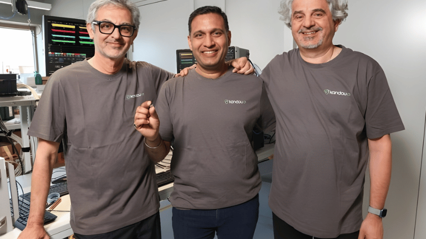
💡$225M for copper beating optics in AI chips: infra shift ahead?
⚡ 30-Second TL;DR
What Changed
$225M Series A funding valuing company at $400M
Why It Matters
Massive funding bolsters copper interconnects as cost-effective alternative to optics, vital for AI datacenter efficiency. Could reshape AI infrastructure supply chains with broader investor backing.
What To Do Next
Evaluate Kandou copper interconnects for AI cluster prototypes to compare vs optical latency/cost.
Key Points
- •$225M Series A funding valuing company at $400M
- •Led by Maverick Silicon with SoftBank, Synopsys participation
- •Focuses on copper chip-to-chip interconnects vs optics
- •Targets AI hardware scaling needs
🧠 Deep Insight
AI-generated analysis for this event — not the original article.
🔑 Enhanced Key Takeaways
- •Kandou's proprietary Chord signaling technology enables high-bandwidth, low-power data transmission over copper, specifically targeting the 'memory wall' bottleneck in AI training clusters.
- •The funding round is earmarked for scaling the production of their 'Glasswing' and 'Matterhorn' IP cores, which are designed to integrate directly into high-performance AI SoCs.
- •Strategic backing from EDA giants Synopsys and Cadence suggests a move toward deep integration of Kandou's interconnect IP into standard semiconductor design flows, potentially accelerating industry-wide adoption.
📊 Competitor Analysis▸ Show
| Feature | Kandou (Copper) | Optical Interconnects (e.g., Ayar Labs) | Traditional SerDes (PCIe/Ethernet) |
|---|---|---|---|
| Latency | Ultra-low (nanoseconds) | Higher (conversion overhead) | Moderate |
| Power Efficiency | High (optimized for short reach) | High (for long reach) | Lower (at high bandwidth) |
| Cost | Lower (CMOS compatible) | High (laser/packaging complexity) | Low (commodity) |
| Reach | Short (Chip-to-Chip) | Long (Rack-to-Rack) | Medium/Long |
🛠️ Technical Deep Dive
- Chord Signaling Technology: Utilizes multi-wire differential signaling to transmit more than one bit per clock cycle, increasing bandwidth density without requiring higher clock frequencies.
- Energy Efficiency: Designed to achieve sub-pJ/bit (picojoules per bit) power consumption, significantly reducing the thermal envelope of high-density AI compute modules.
- Integration: IP cores are optimized for advanced process nodes (5nm, 3nm) to ensure compatibility with leading-edge GPU and TPU architectures.
- Signal Integrity: Advanced equalization techniques allow for reliable data transmission over copper traces at speeds exceeding 100Gbps per lane.
🔮 Future ImplicationsAI analysis grounded in cited sources
⏳ Timeline
Weekly AI Recap
Read this week's curated digest of top AI events →
👉Related Updates


AI-curated news aggregator. All content rights belong to original publishers.
Original source: The Next Web (TNW) ↗
This is a summary, not the original. Read the source, or get the weekly briefing.
Weekly AI briefing
One email a week. Unsubscribe anytime.