JCET Invests $1.15B in New Shanghai Advanced Packaging Plant
💡Major infrastructure expansion for AI chips: JCET's $1.15B investment signals a shift in domestic AI hardware capacity.
⚡ 30-Second TL;DR
What Changed
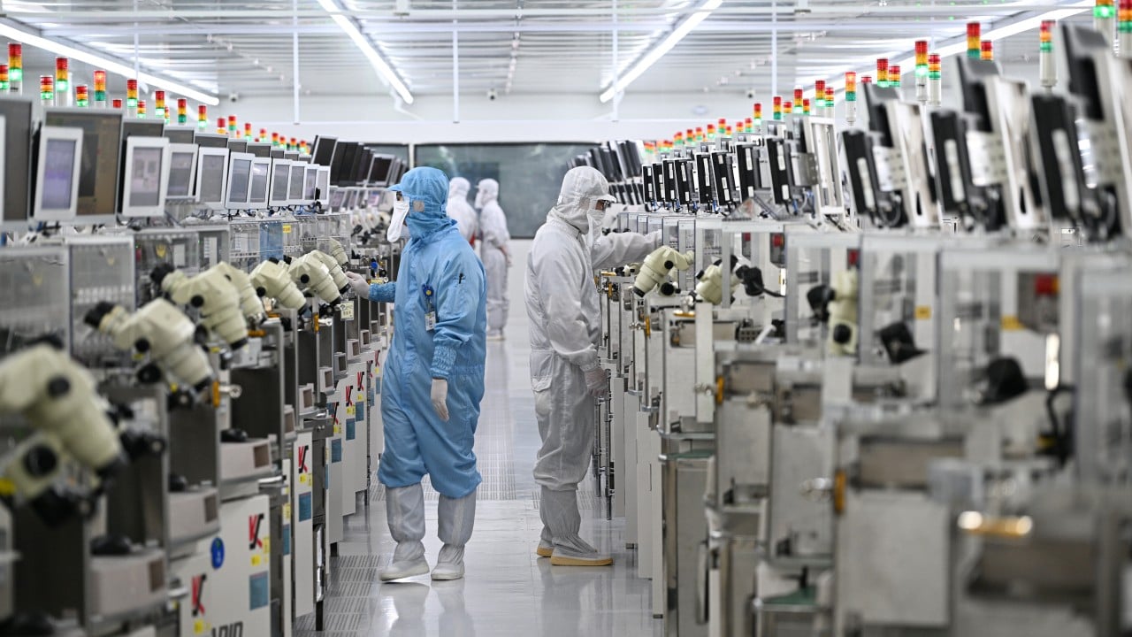
JCET will invest 7.8 billion yuan (US$1.15 billion) in a new Shanghai-based facility.
Why It Matters
This investment strengthens China's domestic semiconductor supply chain, potentially reducing reliance on foreign packaging services for high-performance AI chips. It signals a strategic push to scale local infrastructure for AI hardware production.
What To Do Next
Monitor the availability of domestic advanced packaging capacity if you are sourcing hardware for AI model training or inference in the Chinese market.
🧠 Deep Insight
AI-generated analysis for this event.
🔑 Enhanced Key Takeaways
- •The Lin-gang Special Area facility is strategically positioned to leverage tax incentives and proximity to the Shanghai Free Trade Zone, facilitating easier import of semiconductor manufacturing equipment.
- •This investment aligns with China's 'National Integrated Circuit Industry Investment Fund' (Big Fund) Phase III objectives, which prioritize domestic self-sufficiency in advanced packaging technologies like 2.5D and 3D stacking.
- •JCET has been aggressively expanding its 'XDFOI' (eXtreme Density FOI) chiplet packaging platform, which is expected to be the primary technology deployed at the new Shanghai site.
- •The project is part of a broader trend where Chinese OSAT (Outsourced Semiconductor Assembly and Test) providers are shifting focus toward high-bandwidth memory (HBM) integration to support domestic AI GPU production.
- •The new subsidiary, JCET Semiconductor (Shanghai) Co., Ltd., will integrate R&D and mass production capabilities to shorten the feedback loop between chip design houses and packaging engineers.
📊 Competitor Analysis▸ Show
| Competitor | Primary Advanced Packaging Tech | Market Focus | Key Advantage |
|---|---|---|---|
| ASE Technology | FOCoS, VIPack | Global AI/HPC | Largest global capacity |
| Amkor Technology | SWIFT, SLIM | Automotive/Mobile | US-based supply chain |
| Tongfu Microelectronics | Chiplet/2.5D | Domestic AI/CPU | Deep integration with AMD |
| Powertech Technology | Memory/Logic integration | Memory/HBM | Strong HBM packaging expertise |
🛠️ Technical Deep Dive
- The facility will focus on XDFOI (eXtreme Density FOI) technology, which supports high-density multi-die integration.
- Implementation of TSV (Through-Silicon Via) and TCB (Thermal Compression Bonding) processes to enable high-bandwidth, low-latency interconnects for AI accelerators.
- Support for heterogeneous integration of logic, memory, and I/O dies on a single package substrate.
- Advanced fan-out wafer-level packaging (FOWLP) capabilities to improve thermal management and electrical performance for high-TDP (Thermal Design Power) AI chips.
🔮 Future ImplicationsAI analysis grounded in cited sources
⏳ Timeline
Weekly AI Recap
Read this week's curated digest of top AI events →
👉Related Updates

AI-curated news aggregator. All content rights belong to original publishers.
Original source: SCMP Technology ↗