Intel plans 14A Gen2 process to challenge 1.4nm rivals
💡Crucial updates on the chip manufacturing race that will define the hardware limits of future AI models.
⚡ 30-Second TL;DR
What Changed
Intel is developing the 14A Gen2 process as an evolution of its standard 14A node.
Why It Matters
The foundry war between Intel, TSMC, and Samsung is critical for AI practitioners, as these nodes will dictate the power efficiency and compute density of future AI accelerators and GPUs.
What To Do Next
Monitor Intel Foundry's roadmap updates to assess when these nodes will be available for custom AI silicon tape-outs.
Key Points
- •Intel is developing the 14A Gen2 process as an evolution of its standard 14A node.
- •The move is a direct response to the 1.4nm manufacturing advancements from TSMC and Samsung.
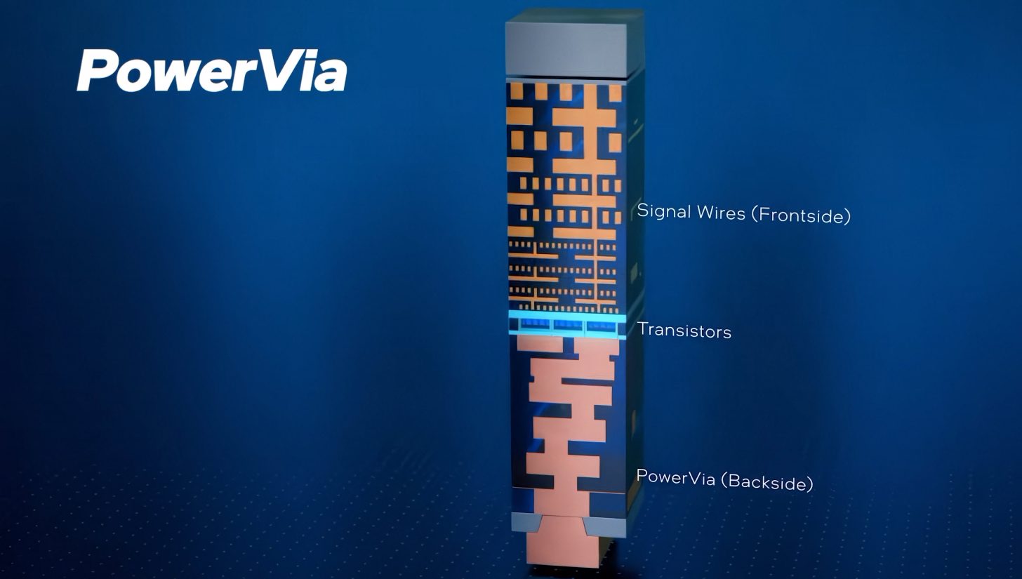
- •Advanced backside power delivery technology is expected to be a key feature of this new node.
🧠 Deep Insight
AI-generated analysis for this event — not the original article.
🔑 Enhanced Key Takeaways
- •Intel's 14A process utilizes High-NA EUV (Extreme Ultraviolet) lithography, which is critical for achieving the resolution required for sub-1.5nm feature sizes.
- •The 14A node family represents Intel's transition to the Angstrom era, moving beyond the 'Intel 18A' node which was previously the company's primary focus for foundry leadership.
- •Intel Foundry (formerly IFS) is positioning 14A Gen2 specifically to attract hyperscaler AI chip designers who require extreme transistor density and power efficiency.
- •The development of 14A Gen2 is integrated into Intel's '5 nodes in 4 years' strategy, serving as the successor to the initial 14A rollout to extend the node's lifecycle.
- •Backside power delivery, branded by Intel as PowerVia, will be further optimized in 14A Gen2 to reduce IR drop and improve signal integrity at higher clock speeds.
📊 Competitor Analysis▸ Show
| Feature | Intel 14A Gen2 | TSMC A14 (1.4nm) | Samsung 1.4nm (SF1.4) |
|---|---|---|---|
| Lithography | High-NA EUV | High-NA EUV | High-NA EUV |
| Power Delivery | Advanced PowerVia | Backside Power Rail | Backside Power Delivery |
| Target Production | ~2027 | ~2027 | ~2027 |
| Primary Focus | AI/HPC Foundry | Mobile/AI/HPC | Mobile/AI/HPC |
🛠️ Technical Deep Dive
- High-NA EUV Integration: Utilizes 0.55 NA optics to enable finer patterning without multi-patterning complexity.
- PowerVia Evolution: Enhanced backside power delivery network (PDN) architecture to decouple power and signal routing, minimizing parasitic resistance.
- Transistor Architecture: Likely utilizes RibbonFET (GAA - Gate-All-Around) structures, which are essential for scaling below 2nm.
- Design Rule Optimization: 14A Gen2 focuses on shrinking standard cell heights to increase logic density compared to the base 14A node.
🔮 Future ImplicationsAI analysis grounded in cited sources
⏳ Timeline
Weekly AI Recap
Read this week's curated digest of top AI events →
👉Related Updates


AI-curated news aggregator. All content rights belong to original publishers.
Original source: cnBeta (Full RSS) ↗
This is a summary, not the original. Read the source, or get the weekly briefing.
Weekly AI briefing
One email a week. Unsubscribe anytime.