⚛️Ars Technica AI•Stalecollected in 1m
Intel Goes All-In on AI Chip Packaging
💡Intel's packaging bet promises denser AI chips—vital for scaling models affordably.
⚡ 30-Second TL;DR
What Changed
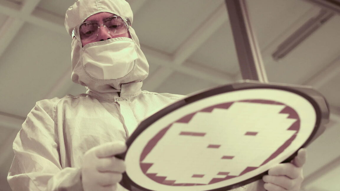
Intel commits entirely to advanced chip packaging
Why It Matters
Intel's push could accelerate AI hardware innovations, offering practitioners more efficient chips for training and inference. It intensifies competition with Nvidia in AI infrastructure.
What To Do Next
Evaluate Intel's advanced packaging roadmap for next AI accelerator procurement.
Who should care:Enterprise & Security Teams
Key Points
- •Intel commits entirely to advanced chip packaging
- •Strategy targets profits from AI boom
- •Focus on packaging for denser, efficient AI chips
🧠 Deep Insight
AI-generated analysis for this event.
🔑 Enhanced Key Takeaways
- •Intel is leveraging its proprietary Foveros 3D packaging technology to integrate heterogeneous chiplets, allowing for the combination of high-bandwidth memory (HBM) and compute tiles on a single package to reduce latency in AI workloads.
- •The strategy involves a significant expansion of Intel's Foundry Services (IFS) capacity, specifically targeting external AI chip designers who require advanced packaging services even if they do not use Intel's primary silicon manufacturing nodes.
- •Intel is shifting away from monolithic die designs for its high-end AI accelerators, adopting a modular 'tile-based' architecture that improves yield rates and allows for faster iteration cycles in response to rapidly evolving AI model requirements.
📊 Competitor Analysis▸ Show
| Feature | Intel (Foveros/EMIB) | TSMC (CoWoS) | Samsung (I-Cube/H-Cube) |
|---|---|---|---|
| Primary Tech | EMIB / Foveros | CoWoS-S/R/L | I-Cube / H-Cube |
| Market Position | Integrated IDM 2.0 | Dominant Foundry | Emerging Foundry |
| AI Focus | High-density chiplet integration | High-volume HBM integration | Custom HBM/Logic integration |
🛠️ Technical Deep Dive
- EMIB (Embedded Multi-die Interconnect Bridge): A high-density, low-cost silicon bridge that connects dies within a package, providing high-bandwidth communication without the need for a full silicon interposer.
- Foveros: A 3D packaging technology that enables face-to-face die stacking, significantly reducing the physical distance between compute and memory components to lower power consumption.
- Omni-Directional Interconnect (ODI): A packaging technology that allows for vertical and horizontal communication between stacked dies, providing greater flexibility in power delivery and signal routing for high-TDP AI chips.
🔮 Future ImplicationsAI analysis grounded in cited sources
Intel Foundry Services will become a primary revenue driver over internal product sales.
By opening advanced packaging to third-party AI chip designers, Intel can monetize its infrastructure regardless of the success of its own AI accelerator product line.
Intel will achieve parity in AI chip performance-per-watt with competitors by 2027.
The transition to modular, tile-based architectures allows Intel to optimize power delivery specifically for AI workloads, mitigating the efficiency losses inherent in monolithic designs.
⏳ Timeline
2018-12
Intel announces Foveros 3D packaging technology at Architecture Day.
2021-03
Intel launches IDM 2.0 strategy, emphasizing the expansion of foundry services and packaging capabilities.
2023-06
Intel reorganizes into internal foundry model to separate product design from manufacturing and packaging.
2024-02
Intel hosts 'Direct Connect' event to detail the roadmap for advanced packaging and foundry expansion.
📰
Weekly AI Recap
Read this week's curated digest of top AI events →
👉Related Updates
AI-curated news aggregator. All content rights belong to original publishers.
Original source: Ars Technica AI ↗