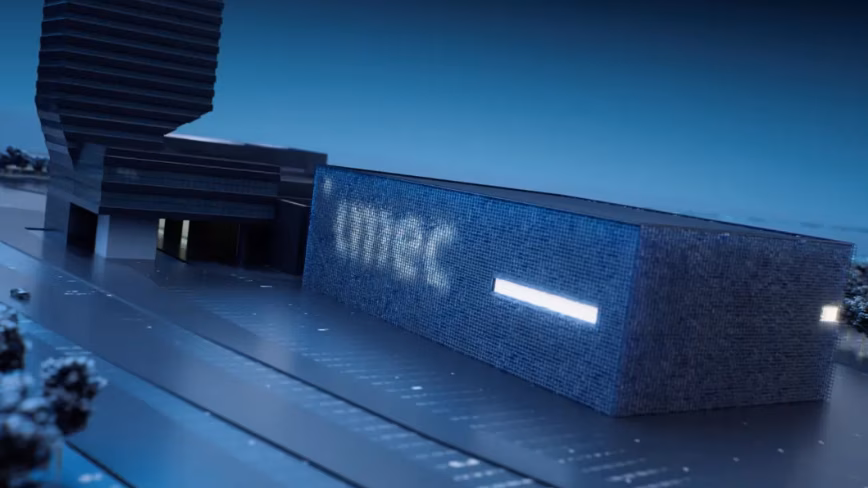
IMEC unveils 325GHz chip platform for 6G
💡Breakthrough in 6G hardware that will define the infrastructure for future high-speed AI edge computing.
⚡ 30-Second TL;DR
What Changed
Platform supports frequencies up to 325GHz
Why It Matters
This research is critical for the future of high-speed AI data transmission and edge computing, enabling faster communication between distributed AI nodes.
What To Do Next
Review IMEC's technical whitepapers on RF silicon interposers to understand how sub-terahertz hardware will impact future AI edge device connectivity.
🧠 Deep Insight
Web-grounded analysis with 13 cited sources.
🔑 Enhanced Key Takeaways
- •The platform integrates high-density metal-insulator-metal (MIM) capacitors using a high-k aluminum-hafnium-oxide dielectric and a three-dimensional oxide-stud architecture, achieving a 10- to 100-fold increase in capacitance density compared to typical on-chip capacitors in III-V processes.
- •It enables heterogeneous integration of performance-critical III-V chiplets (such as InP, GaAs, and GaN) with cost-effective Si-CMOS technology on a single 300mm silicon interposer, allowing III-V dies to focus on active functions while the interposer handles passive components and interconnects.
- •IMEC has developed a scalable passive modeling framework for RF passives on the interposer, validated up to approximately 300 GHz, which allows designers to predict circuit performance based on geometry and layout, thereby shortening design cycles.
- •The platform incorporates laser-assisted bonding for III-V chiplet assembly, achieving high alignment accuracy (below 600nm) and minimal rotational misalignment (below 0.05°) without compromising the thermal integrity of sensitive interposer layers.
- •The technology demonstrates a record-low insertion loss of 0.73dB/mm at frequencies up to 325GHz, which is crucial for unlocking the potential of mmWave and sub-THz frequency bands for 6G and other high-speed applications.
🛠️ Technical Deep Dive
- Interposer Wafer Size: 300 mm RF silicon interposer platform.
- Integrated Passive Components: High-density metal–insulator–metal (MIM) capacitors.
- MIM Dielectric Material: High-k aluminum–hafnium–oxide.
- MIM Structure: Three-dimensional oxide-stud Back-End-of-Line (BEOL) architecture.
- Capacitance Density: 10–100x increase compared to typical on-chip capacitors in III-V processes.
- Heterogeneous Integration: Supports III-V chiplets (InP, GaAs, GaN) on Si-CMOS.
- RF/Microwave Interconnects: 5µm line width and 5µm spacing.
- High-Density Digital Interconnects: 1µm line width and 1µm spacing.
- Flip-Chip Pitch: 40µm, with ongoing efforts to scale down to 20µm.
- Insertion Loss: Record-low 0.73dB/mm at frequencies up to 325GHz.
- Bonding Technique: Laser-assisted bonding for III-V chiplet assembly, achieving alignment accuracy below 600nm and rotational misalignment below 0.05°.
- Passive Modeling Framework: Validated up to approximately 300 GHz, enabling parametric models for transmission lines, inductors, and MIM capacitors.
🔮 Future ImplicationsAI analysis grounded in cited sources
⏳ Timeline
📎 Sources (13)
Factual claims are grounded in the sources below. Forward-looking analysis is AI-generated interpretation.
Weekly AI Recap
Read this week's curated digest of top AI events →
👉Related Updates
Same topic
Explore #6g
Same product
More on imec-6g-chip-platform
Same source
Latest from The Next Web (TNW)
Neuron Soundware launches €150 AI drone detection system

ALS patient uses brain implant to speak with 99% accuracy
Qualcomm launches Snapdragon Reality Elite for AI glasses

Rokarolla Android trojan targets 217 banking and crypto apps
AI-curated news aggregator. All content rights belong to original publishers.
Original source: The Next Web (TNW) ↗