🇨🇳cnBeta (Full RSS)•Stalecollected in 4h
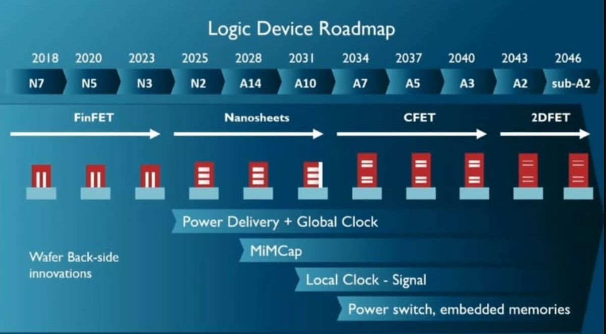
IMEC: Chips Scale to 0.2nm by 2046
💡0.2nm chips by 2046 = decades more cheap AI compute power.
⚡ 30-Second TL;DR
What Changed
Silicon chip processes viable for another 20 years per IMEC
Why It Matters
Prolongs silicon's role in AI hardware, delaying exotic alternatives and enabling denser, cheaper AI chips long-term. Impacts planning for future AI infrastructure investments.
What To Do Next
Download IMEC's full roadmap PDF to inform your AI chip scaling projections.
Who should care:Researchers & Academics
Key Points
- •Silicon chip processes viable for another 20 years per IMEC
- •Roadmap targets sub-0.2nm nodes by 2046
- •Challenges narrative of Moore's Law ending soon
- •Focus on continued scaling despite industry pessimism
🧠 Deep Insight
AI-generated analysis for this event.
🔑 Enhanced Key Takeaways
- •IMEC's roadmap relies heavily on the transition to Forksheet and CFET (Complementary FET) architectures to maintain area scaling beyond the 2nm node.
- •The 0.2nm nomenclature refers to 'effective' scaling rather than physical gate length, as physical dimensions are approaching atomic limits where quantum tunneling dominates.
- •The roadmap emphasizes 'system-technology co-optimization' (STCO), shifting focus from pure transistor density to optimizing the entire chip architecture and packaging to gain performance.
🛠️ Technical Deep Dive
- •Transition from FinFET to Gate-All-Around (GAA) nanosheets is the immediate precursor to advanced nodes.
- •Implementation of CFET (Complementary FET) stacks n-type and p-type transistors vertically to reduce footprint by approximately 50%.
- •Utilization of high-NA EUV (Extreme Ultraviolet) lithography is essential for patterning features at the sub-2nm level.
- •Integration of backside power delivery networks (BSPDN) to decouple power and signal routing, reducing IR drop and improving performance.
🔮 Future ImplicationsAI analysis grounded in cited sources
Foundries will prioritize 3D stacking over 2D planar scaling by 2035.
Physical limitations of silicon at atomic scales make vertical integration the only viable path for continued density improvements.
The cost per transistor will cease to decrease after the 1nm node.
The extreme complexity of manufacturing processes like CFET and high-NA EUV lithography will offset the gains from increased transistor density.
⏳ Timeline
2021-06
IMEC unveils the CFET architecture concept to succeed GAA nanosheets.
2023-05
IMEC presents the 'Beyond 2nm' roadmap at the ITF World conference.
2024-04
IMEC and ASML announce the installation of the first high-NA EUV scanner for sub-2nm research.
📰
Weekly AI Recap
Read this week's curated digest of top AI events →
👉Related Updates
Same topic
Explore #chip-scaling
Same product
More on imec-roadmap
Same source
Latest from cnBeta (Full RSS)
PACA: Open-source tool for ancient fossil coordinate mapping
cnBeta (Full RSS)•Jul 28

First atmosphere detected on habitable-zone exoplanet
cnBeta (Full RSS)•Jul 25

Samsung Secures $200B Broadcom AI Infrastructure Deal
cnBeta (Full RSS)•Jul 25

How AMD's 2006 ATI Acquisition Built Today's AI Empire
cnBeta (Full RSS)•Jul 25
AI-curated news aggregator. All content rights belong to original publishers.
Original source: cnBeta (Full RSS) ↗