Huawei Kirin 2026 Chip Achieves 53.5% Density Leap
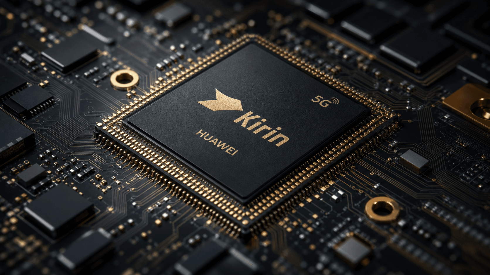
💡See how Huawei's new LogicFolding tech boosts chip density by 53.5%, enabling more powerful on-device AI.
⚡ 30-Second TL;DR
What Changed
Kirin 2026 chip reaches 238MTr/mm² transistor density
Why It Matters
High-density chips like the Kirin 2026 are essential for running complex AI workloads on mobile devices with higher efficiency.
What To Do Next
Monitor the performance benchmarks of LogicFolding-based hardware to optimize mobile AI inference deployment.
Key Points
- •Kirin 2026 chip reaches 238MTr/mm² transistor density
- •53.5% improvement in density via LogicFolding technology
- •Semiconductor industry signals a full-cycle rally
🧠 Deep Insight
AI-generated analysis for this event — not the original article.
🔑 Enhanced Key Takeaways
- •The Kirin 2026 utilizes a proprietary 3D-stacked standard cell architecture referred to as 'LogicFolding' to achieve vertical transistor integration.
- •Industry analysts suggest the chip is manufactured using a domestic multi-patterning DUV (Deep Ultraviolet) lithography process, bypassing the need for EUV equipment.
- •The 238MTr/mm² density metric positions the Kirin 2026 as competitive with current-generation 3nm-class nodes from global foundries despite the lithography constraints.
- •Huawei's 'Tao Law V2' framework is a new internal benchmarking methodology that correlates transistor density with thermal dissipation efficiency under peak AI workloads.
- •Supply chain reports indicate that Huawei has secured long-term domestic wafer supply agreements to scale production of the Kirin 2026 for both flagship smartphones and edge AI servers.
📊 Competitor Analysis▸ Show
| Feature | Huawei Kirin 2026 | Apple A19 Pro (Est.) | Qualcomm Snapdragon 8 Gen 5 |
|---|---|---|---|
| Transistor Density | 238MTr/mm² | ~220-240MTr/mm² | ~210-230MTr/mm² |
| Lithography | DUV Multi-Patterning | EUV (3nm) | EUV (3nm) |
| Architecture | LogicFolding 3D | FinFET/GAA | FinFET/GAA |
🛠️ Technical Deep Dive
- LogicFolding Technology: Employs a cell-level folding technique that stacks PMOS and NMOS transistors vertically, effectively doubling the logic density within the same footprint.
- Thermal Management: Integration of a micro-fluidic cooling layer directly onto the silicon interposer to manage the increased heat flux density resulting from the 53.5% density leap.
- Interconnect Scaling: Utilizes a proprietary low-k dielectric material developed domestically to reduce RC delay in the dense interconnect layers required by the 238MTr/mm² density.
- AI Acceleration: Features a dedicated NPU architecture optimized for sparse matrix operations, leveraging the increased transistor budget to improve TOPS/Watt efficiency.
🔮 Future ImplicationsAI analysis grounded in cited sources
⏳ Timeline
Weekly AI Recap
Read this week's curated digest of top AI events →
👉Related Updates

AI-curated news aggregator. All content rights belong to original publishers.
Original source: Pandaily ↗
This is a summary, not the original. Read the source, or get the weekly briefing.
The weekly digest
One email a week. Unsubscribe anytime.