GeForce 3 Marks 25 Years of GPU Innovation
💡Shader milestone evolved into GPU compute powering AI training
⚡ 30-Second TL;DR
What Changed
GeForce 3 launched on February 27, 2001
Why It Matters
Pioneered programmable GPUs, foundational for modern compute shaders in AI and graphics workloads.
What To Do Next
Review GeForce 3 docs to trace shader evolution to modern AI compute APIs like CUDA.
🧠 Deep Insight
Web-grounded analysis with 8 cited sources.
🔑 Enhanced Key Takeaways
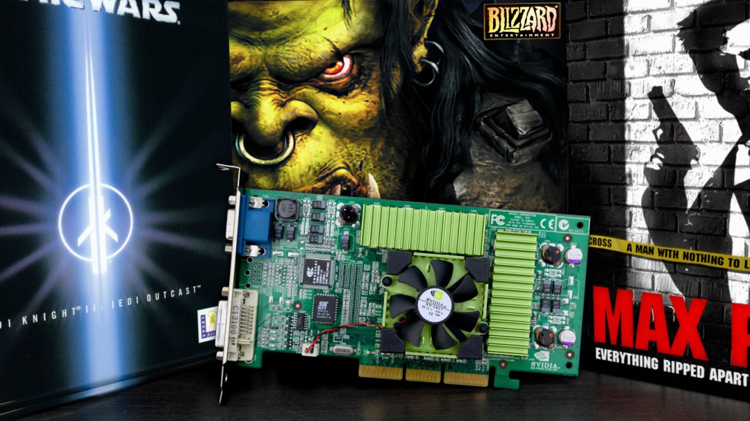
- •The GeForce3 (NV20) contained 57 million transistors built on a 150nm process, exceeding Intel's Pentium 4 CPU transistor count at launch and enabling hardware-accelerated vertex and pixel processing that freed developers from CPU-bound geometry calculations[3][4].
- •GeForce3 introduced Quincunx anti-aliasing technology, which achieved high-quality anti-aliasing by sampling five pixels with only two samples—delivering visual quality comparable to 4x oversampling at twice the performance[3].
- •The architecture supported higher-order surface evaluation (Bézier, B-spline, Catmull-Rom splines) with water-tight tessellation and continuous level-of-detail rendering, enabling real-time patch-based surface rendering without visual popping artifacts[1][3].
- •GeForce3 maintained backward compatibility with DirectX 7.0 through retained fixed-function T&L hardware alongside the new programmable vertex shader, allowing legacy applications to run without performance degradation[2].
📊 Competitor Analysis▸ Show
| Feature | GeForce3 | GeForce2 Ultra | Gloria III | Synergy III |
|---|---|---|---|---|
| Programmable Shaders | Yes (VS 1.1, PS 1.1) | No | No | No |
| Transistor Count | 57M | N/A | N/A | N/A |
| Memory | 64 MB DDR | N/A | N/A | N/A |
| Core Clock (MHz) | 200 | ~250 | N/A | N/A |
| 3ds Max Benchmark (fps) | 45 | N/A | 48 | 42 |
| DirectX Support | 8.0 | 7.0 | N/A | N/A |
🛠️ Technical Deep Dive
- Vertex Shader Architecture: Programmable geometry processor enabling per-vertex operations including deformations (facial animation, skinning), lighting, bump mapping, motion blur, and realistic fur rendering[3]
- Pixel Shader Pipeline: Four pixel pipelines with dual texture sampling per clock cycle; full single-precision floating-point support for per-pixel shading calculations and dependent texture reads[1][2]
- Texture Shaders: Programmable per-pixel shading with dot product operations and dependent texture addressing for effects like true reflective bump mapping[1]
- Memory Architecture: 64 MB DDR memory on 128-bit interface with 8 GB/s bandwidth; Lightspeed Memory Architecture (LMA) optimization[4][6]
- Fabrication: TSMC 150nm process; die size and thermal design requiring dual heatsinks and active cooling[3]
- API Support: DirectX 8.0, OpenGL 1.3; support for 3D textures, shadow buffers, and occlusion culling[2]
🔮 Future ImplicationsAI analysis grounded in cited sources
⏳ Timeline
📎 Sources (8)
Factual claims are grounded in the sources below. Forward-looking analysis is AI-generated interpretation.
Weekly AI Recap
Read this week's curated digest of top AI events →
👉Related Updates
Same topic
Explore #gpu-history
Same product
More on nvidia-geforce-3
Same source
Latest from cnBeta (Full RSS)

PS6 BOM Costs Near $1000, Launch Expected on Schedule

AI Boom Drives Memory Chip Shortages and Price Hikes

Nvidia Leads TSMC CoWoS Capacity Demand Through 2027

US Navy Lab Unveils Portable DNA Threat Detection Device
AI-curated news aggregator. All content rights belong to original publishers.
Original source: cnBeta (Full RSS) ↗