🇨🇳cnBeta (Full RSS)•Stalecollected in 2h
DTU Nano Laser Reshapes Future Chips
💡Thousands of nano lasers per chip could slash AI hardware power needs dramatically.
⚡ 30-Second TL;DR
What Changed
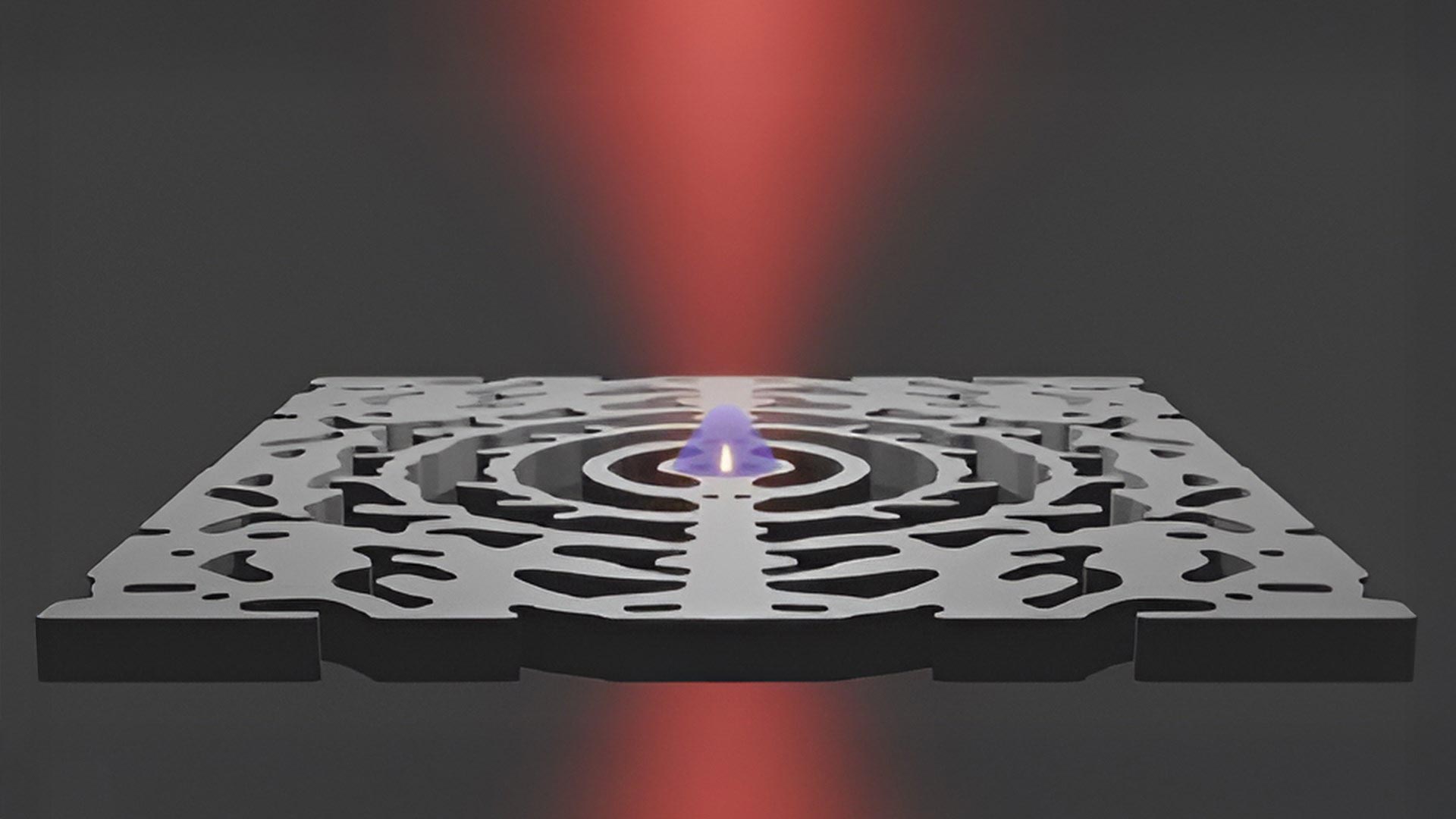
Nano laser constructed in semiconductor thin films by DTU team
Why It Matters
This advances photonic computing, potentially enabling denser AI accelerators with lower power for data centers. It could accelerate scaling of AI training and inference workloads.
What To Do Next
Review DTU's nano laser paper to prototype photonic interconnects for AI chip designs.
Who should care:Researchers & Academics
Key Points
- •Nano laser constructed in semiconductor thin films by DTU team
- •Enables photonic over electronic data transfer inside chips
- •Supports thousands of units per microchip integration
- •Improves speed while reducing power consumption significantly
🧠 Deep Insight
AI-generated analysis for this event.
🔑 Enhanced Key Takeaways
- •The DTU nano laser utilizes a photonic crystal cavity design, which allows for extreme light confinement within a sub-wavelength volume, overcoming the traditional diffraction limit.
- •The research team successfully demonstrated room-temperature continuous-wave operation, a critical hurdle for practical integration into commercial CMOS manufacturing processes.
- •The integration approach leverages a heterogeneous integration technique, bonding III-V semiconductor materials onto silicon-on-insulator (SOI) wafers to combine light-emitting efficiency with silicon's scalability.
🛠️ Technical Deep Dive
- Cavity Type: Photonic crystal nanobeam cavity.
- Material Platform: Indium Phosphide (InP) membrane bonded to Silicon-on-Insulator (SOI).
- Footprint: Sub-micron scale, enabling high-density integration.
- Operating Mode: Continuous-wave (CW) operation at room temperature.
- Coupling: Efficient evanescent coupling to silicon waveguides for on-chip signal routing.
🔮 Future ImplicationsAI analysis grounded in cited sources
Photonic interconnects will replace copper traces for intra-chip communication by 2030.
The ability to integrate thousands of nano lasers directly onto silicon wafers removes the primary bottleneck of energy-intensive electrical data movement.
Data center power consumption will drop by at least 30% due to optical chip-to-chip interconnects.
Replacing electrical signaling with low-power photonic links eliminates the need for power-hungry electrical-to-optical conversions at every stage of data transmission.
⏳ Timeline
2023-05
DTU researchers publish initial findings on high-efficiency light confinement in semiconductor membranes.
2025-02
Successful demonstration of room-temperature continuous-wave operation for the nano laser prototype.
📰
Weekly AI Recap
Read this week's curated digest of top AI events →
👉Related Updates

AI-curated news aggregator. All content rights belong to original publishers.
Original source: cnBeta (Full RSS) ↗