Domestic Semiconductor Equipment's Three-Year Super Cycle
💡Understand the supply chain shifts affecting AI chip production capacity in the Chinese market.
⚡ 30-Second TL;DR
What Changed
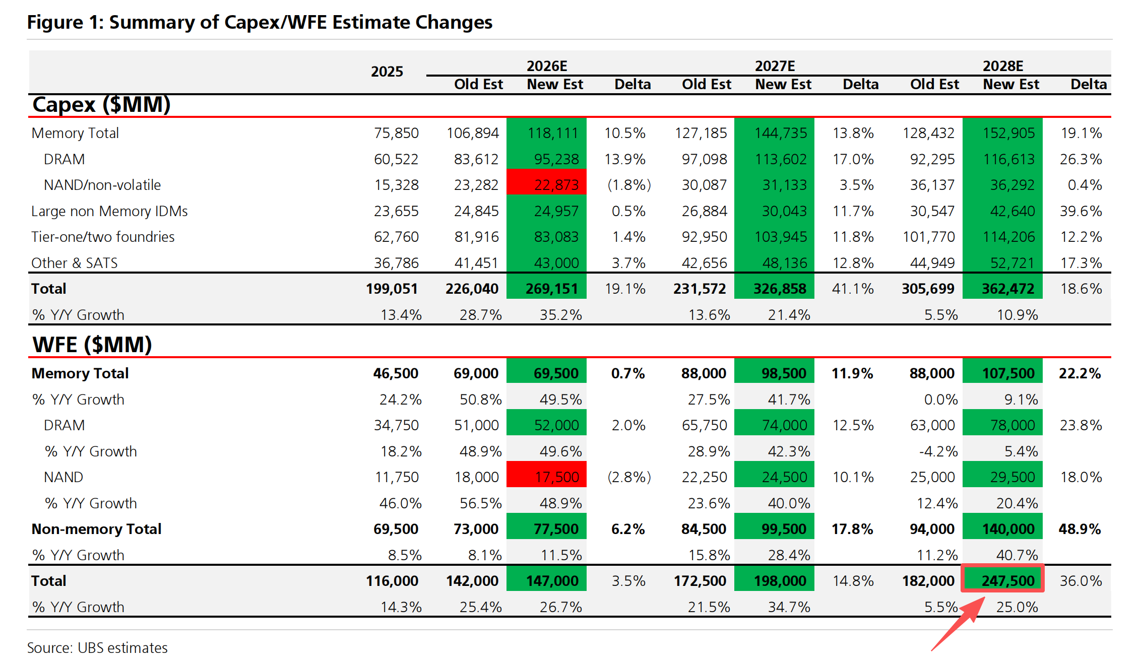
Wafer capacity expansion is driving demand for new equipment.
Why It Matters
Increased local equipment adoption will likely lower supply chain costs for AI chip manufacturers in China. This shift strengthens the domestic infrastructure for AI hardware development.
What To Do Next
Evaluate domestic equipment suppliers for your hardware supply chain to mitigate geopolitical risks.
Key Points
- •Wafer capacity expansion is driving demand for new equipment.
- •Domestic substitution policies are accelerating local adoption.
- •The industry is entering a sustained three-year growth cycle.
🧠 Deep Insight
AI-generated analysis for this event — not the original article.
🔑 Enhanced Key Takeaways
- •The 'super cycle' is heavily underpinned by the transition to advanced packaging technologies, specifically 2.5D and 3D stacking, which require new lithography and etching equipment suites.
- •Chinese semiconductor equipment manufacturers are increasingly focusing on the 28nm and 14nm process nodes, where domestic tool maturity has reached a critical inflection point for mass production.
- •Supply chain resilience initiatives have led to a 'dual-vendor' strategy among major Chinese foundries, forcing a shift from reliance on international incumbents like Applied Materials and Lam Research.
- •Government-backed 'Big Fund' Phase III has shifted its investment focus from basic manufacturing capacity to specialized equipment sub-sectors, including ion implantation and chemical mechanical polishing (CMP).
- •The growth cycle is being amplified by the rapid integration of AI-specific chip architectures, which demand higher volumes of specialized memory and logic wafer starts.
📊 Competitor Analysis▸ Show
| Feature | Domestic Equipment (China) | International Incumbents (AMAT/Lam/ASML) |
|---|---|---|
| Process Node Maturity | 28nm - 14nm (High Volume) | Sub-3nm (Leading Edge) |
| Pricing | Highly Competitive (Cost-Optimized) | Premium (R&D Intensive) |
| Market Access | Protected/Subsidized | Global/Restricted (Export Controls) |
| Technical Support | Localized/Rapid Response | Global/Standardized |
🛠️ Technical Deep Dive
- Etching Equipment: Transitioning from CCP (Capacitively Coupled Plasma) to ICP (Inductively Coupled Plasma) for higher aspect ratio features in 3D NAND and FinFET structures.
- Lithography: Development of DUV (Deep Ultraviolet) immersion systems utilizing multi-patterning techniques to circumvent the lack of EUV access.
- Deposition: Increased adoption of ALD (Atomic Layer Deposition) tools to achieve precise thin-film uniformity required for advanced logic nodes.
- Metrology: Integration of AI-driven optical inspection systems to improve yield rates during the transition to domestic equipment lines.
🔮 Future ImplicationsAI analysis grounded in cited sources
⏳ Timeline
Weekly AI Recap
Read this week's curated digest of top AI events →
👉Related Updates

AI-curated news aggregator. All content rights belong to original publishers.
Original source: 钛媒体 ↗
This is a summary, not the original. Read the source, or get the weekly briefing.
Weekly AI briefing
One email a week. Unsubscribe anytime.