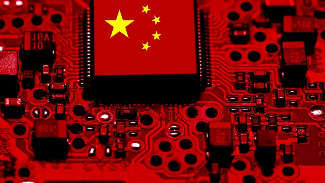
Chinese Startup Bets on 3D Stacking to Bypass US Controls
💡Learn how Chinese firms are using 3D stacking to bypass US chip sanctions and maintain AI compute capabilities.
⚡ 30-Second TL;DR
What Changed
Dongfang Suanxin officially launched its corporate presence to compete in the AI chip market.
Why It Matters
This development highlights the growing reliance on advanced packaging techniques like 3D stacking to maintain AI compute performance in restricted markets. It may lead to a shift in supply chain dynamics for AI hardware developers operating within China.
What To Do Next
Monitor the performance benchmarks of 3D-stacked chips from Chinese manufacturers to assess if they can serve as viable alternatives for non-US-restricted AI workloads.
🧠 Deep Insight
AI-generated analysis for this event.
🔑 Enhanced Key Takeaways
- •Dongfang Suanxin is reportedly leveraging hybrid bonding technology, a critical advanced packaging technique that allows for higher interconnect density than traditional micro-bumping.
- •The company's strategy aligns with China's 'National Integrated Circuit Industry Investment Fund' (Big Fund III) focus on supporting domestic firms that prioritize heterogeneous integration to overcome lithography tool shortages.
- •Wei Shaojun, while leading the startup, maintains his influential role as a professor at Tsinghua University, bridging the gap between academic research in reconfigurable computing and commercial chip production.
- •Industry analysts suggest the startup is targeting the 'Chiplet' ecosystem, aiming to integrate domestically produced logic dies with high-bandwidth memory (HBM) alternatives to circumvent HBM export bans.
- •The startup has secured initial backing from regional government-backed venture capital funds in Beijing, reflecting a localized funding model common among Chinese firms attempting to bypass federal-level investment scrutiny.
📊 Competitor Analysis▸ Show
| Feature | Dongfang Suanxin | Cambricon | Huawei Ascend |
|---|---|---|---|
| Primary Strategy | 3D Stacking/Chiplets | ASIC/NPU Architecture | Full-stack AI Ecosystem |
| Manufacturing | Domestic Advanced Packaging | SMIC 7nm/5nm | SMIC/Domestic Foundries |
| Market Focus | High-Performance AI Training | Edge/Cloud AI Inference | Data Center/Large Models |
🛠️ Technical Deep Dive
- Utilizes 3D heterogeneous integration to stack logic and memory dies, reducing data movement latency and power consumption.
- Employs wafer-to-wafer (W2W) or die-to-wafer (D2W) hybrid bonding to achieve sub-micron interconnect pitches.
- Focuses on reconfigurable computing architectures that allow hardware to adapt to different AI model requirements without needing a full tape-out for every iteration.
- Implements proprietary thermal management solutions to address the heat dissipation challenges inherent in high-density 3D stacked AI chips.
🔮 Future ImplicationsAI analysis grounded in cited sources
⏳ Timeline
Weekly AI Recap
Read this week's curated digest of top AI events →
👉Related Updates

AI-curated news aggregator. All content rights belong to original publishers.
Original source: SCMP Technology ↗