🇨🇳cnBeta (Full RSS)•Stalecollected in 20h
Chinese HBM3e Hits 960GB/s for Sub-3nm AI Chips
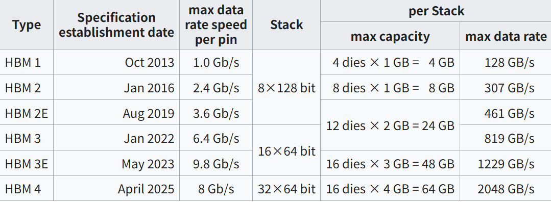
💡960GB/s domestic HBM3e eyes sub-3nm AI chips, easing supply chains
⚡ 30-Second TL;DR
What Changed
960GB/s bandwidth capability
Why It Matters
Advances China's AI hardware self-sufficiency, potentially lowering costs for AI training/inference via high-bandwidth memory alternatives.
What To Do Next
Assess HBM3e specs from Chinese vendors for your next AI accelerator prototype's memory bandwidth needs.
Who should care:Enterprise & Security Teams
🧠 Deep Insight
AI-generated analysis for this event.
🔑 Enhanced Key Takeaways
- •The development utilizes a hybrid bonding process (likely TSV-based) to achieve the 960GB/s bandwidth, marking a significant shift from traditional micro-bump interconnects in Chinese domestic memory production.
- •This HBM3e solution is specifically optimized for integration with domestic Chinese AI accelerators using CoWoS-like (Chip-on-Wafer-on-Substrate) 2.5D packaging, addressing a critical bottleneck in the domestic semiconductor supply chain.
- •Industry analysts note that while 960GB/s matches standard HBM3e specifications, the primary innovation lies in the yield stabilization of the vertical stack using domestic silicon interposers, which previously suffered from high thermal throttling issues.
📊 Competitor Analysis▸ Show
| Feature | Chinese HBM3e | SK Hynix HBM3e | Micron HBM3e |
|---|---|---|---|
| Bandwidth | 960 GB/s | 1.2 TB/s | 1.2 TB/s |
| Process Node | Domestic (Sub-3nm compatible) | 10nm-class (1b) | 10nm-class (1β) |
| Primary Market | Domestic Chinese AI | Global Hyperscalers | Global Hyperscalers |
🛠️ Technical Deep Dive
- Architecture: 8-high (8H) DRAM die stack configuration.
- Interconnect: Utilizes advanced Through-Silicon Vias (TSV) with a pitch optimized for high-density integration on 3nm logic dies.
- Thermal Management: Integrated thermal dissipation layer designed to handle the high power density of sub-3nm AI processors.
- Interface: Compliant with JEDEC HBM3e standards to ensure compatibility with existing memory controllers.
🔮 Future ImplicationsAI analysis grounded in cited sources
Domestic Chinese AI chip production will increase by 20% by Q4 2026.
The availability of locally sourced HBM3e removes the primary supply chain constraint currently limiting the volume production of high-end domestic AI accelerators.
Chinese memory manufacturers will initiate pilot production of HBM4 by early 2027.
Achieving stability in HBM3e manufacturing provides the necessary process maturity and intellectual property foundation to transition to the next generation of HBM standards.
⏳ Timeline
2024-09
Initial announcement of domestic HBM development roadmap by Chinese memory consortium.
2025-05
Successful laboratory validation of TSV stacking technology for high-bandwidth memory.
2026-01
Completion of pilot production line for HBM3e memory modules.
📰
Weekly AI Recap
Read this week's curated digest of top AI events →
👉Related Updates

AI-curated news aggregator. All content rights belong to original publishers.
Original source: cnBeta (Full RSS) ↗