China launches photonics lab to bypass US chip curbs
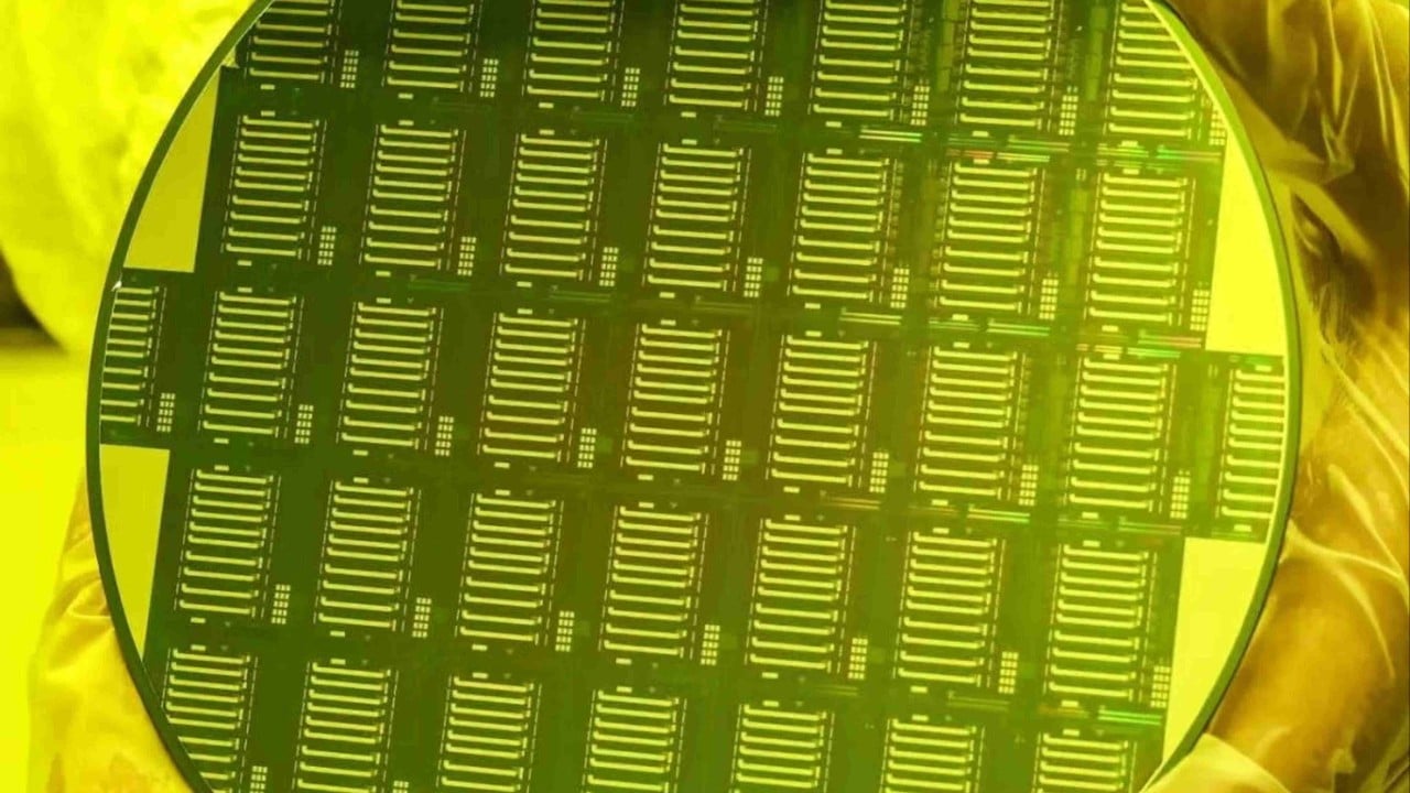
💡China's pivot to photonic computing could disrupt the AI hardware supply chain and bypass current GPU bottlenecks.
⚡ 30-Second TL;DR
What Changed
Launch of the Shanghai Key Laboratory of Integrated Photonic Computing Chips and Systems.
Why It Matters
This development signals a shift toward alternative computing architectures in China, potentially reducing reliance on high-end GPUs like Nvidia's for specific AI workloads.
What To Do Next
Monitor the research outputs from this lab for potential breakthroughs in optical neural network architectures that could redefine AI hardware efficiency.
Key Points
- •Launch of the Shanghai Key Laboratory of Integrated Photonic Computing Chips and Systems.
- •Focus on photonic computing to bypass traditional electronic chip constraints.
- •Strategic move to sustain AI development amid US technology export curbs.
🧠 Deep Insight
Background and context from public sources — not the original article. 13 sources cited.
🔑 Enhanced Key Takeaways
- •The newly established Shanghai Key Laboratory of Integrated Photonic Computing Chips and Systems is linked to the Institute of Photonic Chips (IPC), which was founded in 2021 and is led by Professor Min Gu, with a focus on optically-driven artificial intelligence.
- •China's strategic pivot to photonic computing is a direct response to US restrictions on advanced microchips, GPUs, and Extreme Ultraviolet (EUV) lithography, aiming to achieve energy-efficient AI and potentially 'change lanes and overtake' in technology development.
- •Significant advancements in China include Tsinghua University's 'Taichi' photonic chip, which boasts 160 TOPS/W energy efficiency with a diffractive-interferential architecture, and the Shanghai Institute of Optics and Fine Mechanics' ultra-high parallel optical computing chip, capable of 2560 TOPS at a 50 GHz optical clock speed using soliton microcomb sources for over 100 wavelength channels.
- •Another key facility, CHIPX (Chip Hub for Integrated Photonics Xplore) at Shanghai Jiao Tong University, commenced manufacturing 6-inch thin-film lithium niobate photonic wafers in September 2024, with an annual capacity of 12,000 wafers.
- •Chinese efforts in photonic chip development are also exploring alternative manufacturing processes like nanoimprint lithography, which could reduce production costs by approximately 90% compared to traditional Deep Ultraviolet (DUV)-based processes and bypass the need for advanced DUV/EUV lithography machines restricted by the US.
🛠️ Technical Deep Dive
- Photonic computing leverages photons instead of electrons for data processing, offering fundamental advantages such as reduced heat generation, increased bandwidth, and lower signal losses compared to traditional electronic chips.
- Opto-electronic hybrid chips represent a transitional architecture, utilizing photonics for high-speed data movement and specific operations like matrix multiplication in AI, while retaining electronics for nonlinear functions and memory access.
- Key technical challenges for achieving fully all-optical computing include integrating robust optical memory solutions, as current optical memory materials have limited write cycles, and effectively implementing nonlinear operations.
- Analog optical computing can exploit multiple physical dimensions of light simultaneously (e.g., amplitude, phase, polarization, wavelength) to perform complex operations, such as matrix multiplication, in a single physical step with minimal energy consumption.
- Photonic Integrated Circuits (PICs) integrate various optical components, including laser diodes, waveguides, and filters, onto a single substrate, commonly silicon, silicon nitride (SiN), or indium phosphide (InP), enabling compact and scalable designs.
- The ultra-high parallel optical computing chip developed by the Shanghai Institute of Optics and Fine Mechanics utilizes soliton microcomb sources to generate over 100 distinct wavelength channels, facilitating high-density, 100-wavelength multiplexing for parallel data processing.
- Nanoimprint lithography is being investigated as a manufacturing method for photonic chips, potentially offering a 90% cost reduction over conventional DUV lithography and eliminating the reliance on advanced EUV lithography equipment.
🔮 Future ImplicationsAI analysis grounded in cited sources
⏳ Timeline
📎 Sources (13)
Factual claims are grounded in the sources below. Forward-looking analysis is AI-generated interpretation.
Weekly AI Recap
Read this week's curated digest of top AI events →
👉Related Updates

AI-curated news aggregator. All content rights belong to original publishers.
Original source: SCMP Technology ↗
This is a summary, not the original. Read the source, or get the weekly briefing.
The weekly digest
One email a week. Unsubscribe anytime.