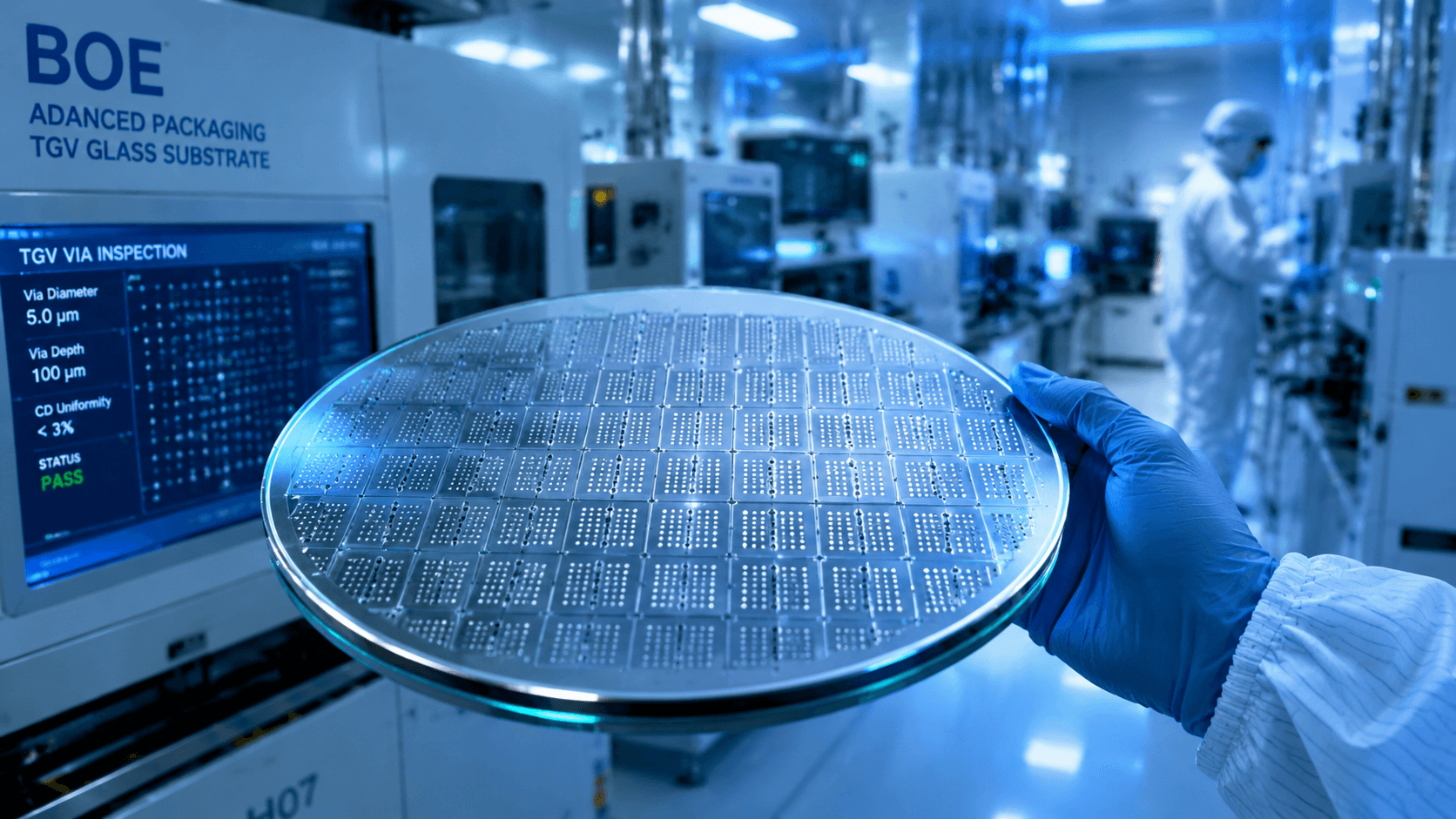
BOE Samples Glass-Based Substrates for Advanced Chip Packaging
💡Glass substrates are the next bottleneck for AI chip performance; track BOE's progress in this critical infrastructure.
⚡ 30-Second TL;DR
What Changed
BOE is developing glass-based carrier substrates for advanced chip packaging.
Why It Matters
Glass substrates are critical for next-gen AI chips, offering better thermal stability and higher interconnect density compared to traditional organic substrates.
What To Do Next
Monitor the supply chain shift toward glass substrates as they will likely become the standard for high-bandwidth AI hardware in the coming years.
🧠 Deep Insight
AI-generated analysis for this event.
🔑 Enhanced Key Takeaways
- •BOE is leveraging its extensive expertise in glass-based display manufacturing (TFT-LCD/OLED) to pivot into semiconductor packaging, utilizing existing glass processing capabilities to reduce substrate costs.
- •The shift to glass substrates is driven by the industry's need for better thermal stability and electrical performance compared to traditional organic substrates in high-performance computing (HPC) and AI chipsets.
- •BOE's glass substrate initiative is part of a broader strategic move to diversify beyond display panels into the semiconductor materials and equipment ecosystem.
- •The transition to glass substrates addresses the 'warpage' issues commonly associated with large-area organic substrates used in advanced packaging like Chip-on-Wafer-on-Substrate (CoWoS).
- •BOE is collaborating with domestic Chinese semiconductor design houses to ensure the glass substrates meet the specific signal integrity requirements for next-generation AI accelerators.
📊 Competitor Analysis▸ Show
| Feature | BOE (Glass Substrate) | Intel (Glass Substrate) | Samsung Electro-Mechanics |
|---|---|---|---|
| Status | Technical Testing | Pilot Line Production | R&D / Pilot Phase |
| Primary Focus | Display-to-Semiconductor Pivot | HPC / Data Center | Mobile / Memory Packaging |
| Key Advantage | Cost-effective glass processing | Established ecosystem/IP | Advanced flip-chip expertise |
🛠️ Technical Deep Dive
- Material Composition: Utilizes high-rigidity borosilicate or specialized display-grade glass to minimize thermal expansion (CTE) mismatch with silicon dies.
- Interconnect Density: Supports finer pitch routing (sub-10 micron) compared to traditional organic substrates, enabling higher I/O density for chiplets.
- Thermal Management: Glass substrates offer superior thermal conductivity and flatness, allowing for more efficient heat dissipation in high-TDP (Thermal Design Power) AI chips.
- Processing: Leverages existing glass-via (TGV) technology, which involves laser drilling and metallization to create vertical electrical connections through the glass layer.
🔮 Future ImplicationsAI analysis grounded in cited sources
⏳ Timeline
Weekly AI Recap
Read this week's curated digest of top AI events →
👉Related Updates


AI-curated news aggregator. All content rights belong to original publishers.
Original source: Pandaily ↗