Apple May Restart YMTC NAND for China iPhones
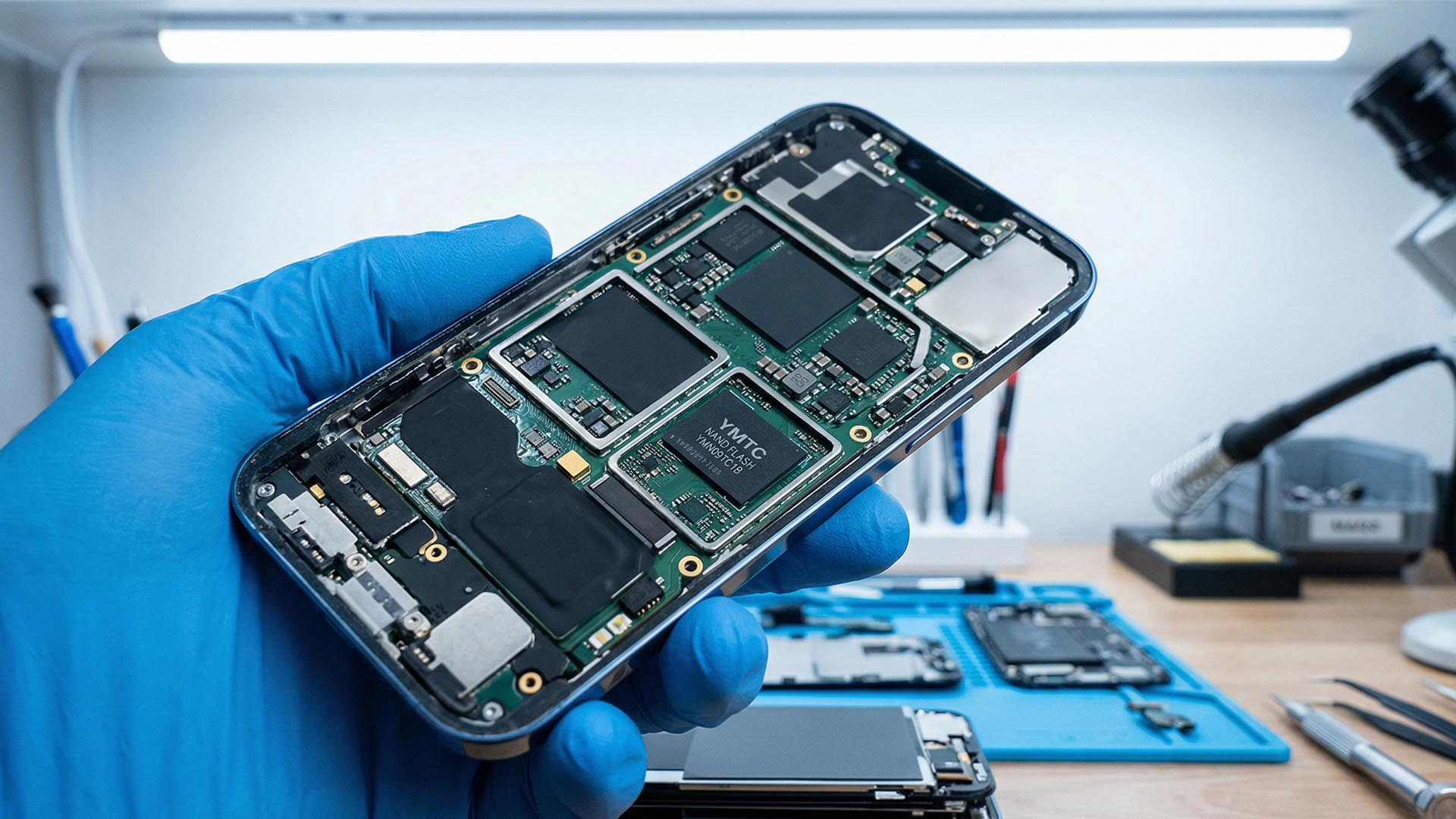
💡Memory price surge hits AI hardware—Apple's YMTC pivot offers supply chain lessons
⚡ 30-Second TL;DR
What Changed
Apple halted YMTC cooperation due to US export controls
Why It Matters
Reduces Apple's supply chain risks and costs, potentially stabilizing iPhone pricing in China. Signals broader memory crunch affecting AI infra hardware budgets.
What To Do Next
Evaluate YMTC NAND specs for cost-optimized storage in AI edge devices.
Key Points
- •Apple halted YMTC cooperation due to US export controls
- •Global NAND and DRAM prices surging, 12GB LPDDR5X at $70
- •Relaunch planned for China iPhone models using domestic NAND
- •Aims to cut costs amid Korean supplier dependency
🧠 Deep Insight
AI-generated analysis for this event — not the original article.
🔑 Enhanced Key Takeaways
- •YMTC has made significant strides in 3D NAND scaling, reportedly achieving 232-layer and 300-layer architectures using its proprietary Xtacking 3.0/4.0 technology, which allows for higher density and performance comparable to Tier-1 suppliers.
- •The potential resumption of the partnership is reportedly contingent on YMTC utilizing non-restricted manufacturing equipment or domestic alternatives to bypass US Bureau of Industry and Security (BIS) Entity List restrictions that previously forced Apple to pause the relationship.
- •Market analysts suggest that Apple's move is part of a broader 'China-for-China' supply chain strategy, aiming to insulate the Chinese iPhone market from potential future geopolitical supply shocks and to leverage local government subsidies that lower YMTC's cost structure.
📊 Competitor Analysis▸ Show
| Feature | YMTC (3D NAND) | Samsung (V-NAND) | Micron (G8/G9 NAND) |
|---|---|---|---|
| Architecture | Xtacking (Hybrid Bonding) | CTF (Charge Trap Flash) | CMOS-under-Array |
| Layer Count | 232L / 300L+ | 236L / 300L+ | 232L / 300L+ |
| Market Position | Value/Domestic Focus | Premium/Global Leader | Premium/Global Leader |
| Geopolitical Risk | High (US Sanctions) | Low | Low |
🛠️ Technical Deep Dive
- Xtacking Architecture: YMTC's core technology involves bonding the CMOS peripheral circuitry and the NAND array wafer separately, then connecting them via vertical interconnect access (VIA) holes, which allows for higher I/O speeds and smaller die sizes.
- 3D NAND Scaling: YMTC has successfully transitioned from 128-layer to 232-layer and beyond, utilizing high-aspect-ratio etching processes that were previously considered a bottleneck for Chinese manufacturers.
- Interface Standards: YMTC's latest NAND chips support ONFI 5.0 standards, enabling data transfer rates of up to 2400 MT/s, aligning them with the performance requirements of modern mobile SoCs.
🔮 Future ImplicationsAI analysis grounded in cited sources
⏳ Timeline
Weekly AI Recap
Read this week's curated digest of top AI events →
👉Related Updates
AI-curated news aggregator. All content rights belong to original publishers.
Original source: cnBeta (Full RSS) ↗
This is a summary, not the original. Read the source, or get the weekly briefing.
The weekly digest
One email a week. Unsubscribe anytime.