AI HBM Demand Surges, 60% Short to 2027
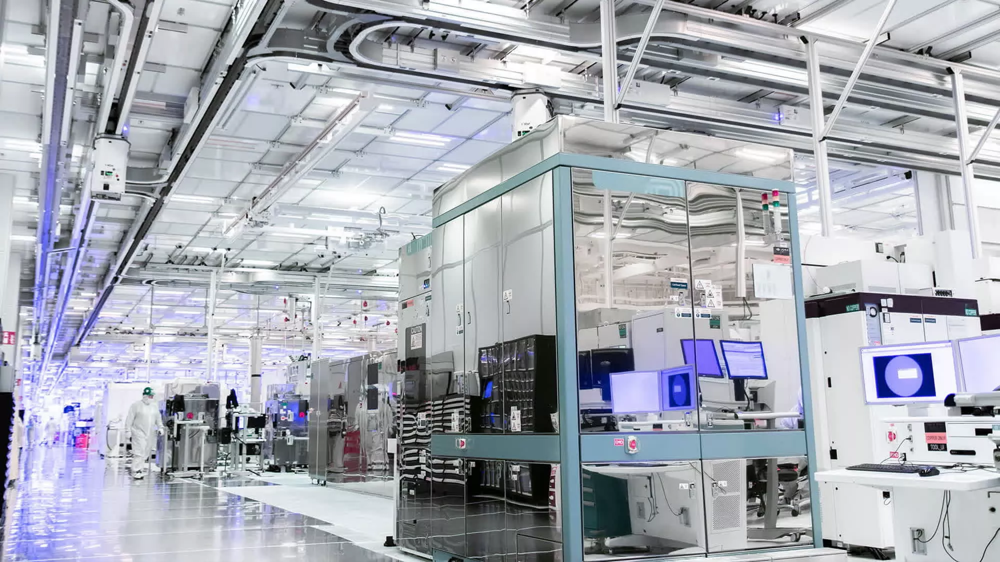
💡HBM shortage to 2027 hikes AI infra costs—secure supply now or face delays.
⚡ 30-Second TL;DR
What Changed
GenAI drives sharp HBM demand growth
Why It Matters
Persistent HBM shortages will raise costs and delay AI model training/deployments for practitioners scaling infrastructure. Companies may need alternative memory tech or stockpiling strategies.
What To Do Next
Contact SK Hynix or Samsung for HBM allocation waitlists to secure supply.
Key Points
- •GenAI drives sharp HBM demand growth
- •Chip makers expanding production full throttle
- •2027 supply covers only 60% of market demand
- •AI consumes entire memory market share
🧠 Deep Insight
AI-generated analysis for this event — not the original article.
🔑 Enhanced Key Takeaways
- •The HBM supply-demand gap is exacerbated by the transition to HBM3E and the upcoming HBM4 standards, which require significantly more complex TSV (Through-Silicon Via) packaging processes.
- •Major memory manufacturers are shifting capital expenditure away from legacy DRAM and NAND production lines to prioritize HBM capacity, leading to potential supply tightness in commodity memory sectors.
- •The industry is seeing a shift toward 'custom HBM' solutions, where memory vendors collaborate directly with logic chip designers (like NVIDIA or AMD) to optimize memory stacks for specific AI accelerator architectures.
📊 Competitor Analysis▸ Show
| Feature | SK Hynix (HBM3E) | Samsung (HBM3E) | Micron (HBM3E) |
|---|---|---|---|
| Market Position | Current Market Leader | Aggressive Capacity Expansion | Focused on Power Efficiency |
| Technology | MR-MUF Packaging | TC-NCF Packaging | 1-beta Node Process |
| Status | High-volume production | Qualifying for major OEMs | Ramping production |
🛠️ Technical Deep Dive
- HBM3E utilizes 8-high or 12-high stacks of DRAM dies connected via TSVs to achieve bandwidths exceeding 1.2 TB/s per stack.
- The transition to HBM4 is expected to move from a 1024-bit wide interface to a 2048-bit interface, necessitating a shift to 12nm or smaller process nodes for the base logic die.
- Thermal management has become a critical bottleneck, leading to the adoption of advanced thermal compression bonding and specialized underfill materials to prevent die warping during the stacking process.
🔮 Future ImplicationsAI analysis grounded in cited sources
⏳ Timeline
Weekly AI Recap
Read this week's curated digest of top AI events →
👉Related Updates
AI-curated news aggregator. All content rights belong to original publishers.
Original source: cnBeta (Full RSS) ↗
This is a summary, not the original. Read the source, or get the weekly briefing.
The weekly digest
One email a week. Unsubscribe anytime.