🇨🇳cnBeta (Full RSS)•較早收集於 2h
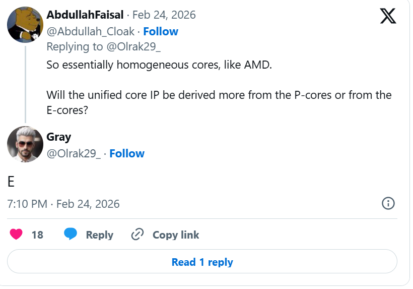
Intel統一CPU大小核:P核消失E核大放光芒
💡Intel CPU redesign favors E-cores for efficient AI inference—watch for server impacts
⚡ 30-Second TL;DR
有什麼變化
招聘貼文曝光Intel統一核心策略
為什麼重要
統一核心可簡化Intel CPU上的AI軟體最佳化,提升E核推論效率。或改變伺服器設計,避開混合複雜性。
下一步行動
Review Intel's oneAPI for E-core optimizations in your CPU-based AI inference workloads.
誰應關注:Developers & AI Engineers
關鍵要點
- •招聘貼文曝光Intel統一核心策略
- •捨棄P核,強調12代後E核
- •無細節/官方回應;產品遙遙無期
- •P+E混合設計優缺眾所周知
🧠 深度解析
背景與延伸:來自公開資料,非原文內容。引用 6 個來源。
🔑 增強重點摘要
- •Intel's Unified Core design uses the same general core architecture and IP for P-cores, E-cores, and LP E-cores, differentiated primarily by power curves rather than entirely separate designs.[1]
- •The Unified Core is reportedly based on an evolution of Intel's efficiency-focused E-cores, which in Darkmont variants already outperform Raptor Cove P-cores at equivalent power levels.[1]
- •First leaks about Unified Core emerged in mid-July 2025, with speculation linking it to Jim Keller’s Royal Core Project and potential use in Titan Lake processors around 2028.[2]
📊 競品分析▸ Show
| Feature | Intel Unified Core | AMD Zen 5/Zen 5c |
|---|---|---|
| Core Design | Same architecture/IP for P/E/LP-E, tuned by power curve | Same microarchitecture/IPC, differ in size/clock speeds |
| Base Focus | E-core evolution for scalability | Unified Zen cores for hybrid-like setups |
| Benchmarks | No data yet (pre-silicon) | Zen 5 competitive in single/multi-thread [5] |
🛠️ 技術深入
- •Unified Core employs a single scalable architecture across core types (P, E, LP-E), with variations in allowed power consumption: highest for P-cores, moderate for E-cores, lowest for LP-E-cores.
- •Likely mimics AMD's Zen 5/Zen 5c approach, sharing microarchitecture and instructions-per-clock (IPC), but tuned for performance vs. density/efficiency.
- •Potentially enables scalability from entry-level client CPUs to datacenter processors, possibly integrating with Intel's 'Software Defined Supercore' for many small cores.
🔮 前景展望AI analysis grounded in cited sources
Intel Unified Core products launch no earlier than 2029
Job postings for verification engineers indicate pre-silicon stages, with tape-out needed by mid-2026 for 2028 launch unlikely, pushing realistic debut to 2029-2030.[2]
Simplified scheduling reduces OS overhead vs. hybrid P+E
Single core type eliminates task distribution complexity between dissimilar P and E cores, similar to AMD's unified Zen approach.[3]
E-core foundation boosts efficiency-per-area ratio
Basing design on advanced E-cores like Darkmont, which match or exceed P-core performance at same power, allows denser, more efficient dies.[1]
⏳ 時間線
2021-10
Alder Lake launches Intel's hybrid P+E core architecture publicly.
2025-07
First leaks emerge about Unified Core, speculated for Titan Lake.
2026-02
Intel job posting for Unified Core verification engineer confirms active development.
📎 來源 (6)
Factual claims are grounded in the sources below. Forward-looking analysis is AI-generated interpretation.
- notebookcheck.net — Intel to Take Page Out of Amd S Book for Next Gen Cpus Using Unified Core Design.1233597.0
- Tom's Hardware — Intel Preps Cpus with Unified Core Architecture Job Listing Hints at Evolution Beyond Intels Hybrid Design
- windowscentral.com — Intel Unified Core Job Listing Rumors
- semiwiki.com — Rumours Around Intels Unified Core Future Chip Designs Are Swirling Once More
- youtube.com — Watch
- techspot.com — 111438 Intel Mysterious Unified Core Team Hints Major Cpu
📰
AI 週報
閱讀本週精選 AI 大事摘要 →
👉相關動態

AI 策展新聞聚合。所有內容版權歸原始發布者所有。
原始來源: cnBeta (Full RSS) ↗
每週 AI 簡報
每週一封,可隨時退訂。